
Lesson 10: Introduction to the GPIO Port Control Register (GPIOPCTL)
What the GPIOPCTL Register Is
Every GPIO port on the TM4C123G and TM4C1294 owns one 32-bit GPIOPCTL register, located at offset 0x52C inside that port's register block. Its job is simple to state but easy to get wrong: it decides which peripheral signal a pin carries when the pin is switched out of plain-GPIO mode.
GPIOPCTL never works alone. It is the second half of a two-step handshake with the GPIOAFSEL (Alternate Function Select) register:
- GPIOAFSEL answers the yes/no question: "Is this pin a plain GPIO, or an alternate function?" (0 = GPIO, 1 = alternate function).
- GPIOPCTL answers the follow-up: "If it's an alternate function, then which one?"
A pin like PA6 can physically be routed to I2C1SCL, M1PWM2, and several other blocks. AFSEL only opens the door to "not-GPIO"; GPIOPCTL is what actually selects I2C1SCL versus M1PWM2. On both chips the reset value is 0x0000.0000, and because AFSEL also resets to 0, every ordinary pin comes up as a plain GPIO.
When Do You Use It?
Use GPIOPCTL only when a pin must act as a digital peripheral signal — for example:
- UART: U0Rx / U0Tx
- SSI / SPI: SSI0Clk, SSI0Rx, SSI0Tx
- I2C: I2C0SCL, I2C0SDA
- PWM: M0PWM0, M1PWM5 …
- Timer capture/compare: T0CCP0, WT2CCP1 …
- CAN, QEI (PhA/PhB/IDX), etc.
You do not touch GPIOPCTL when:
- The pin is a normal digital input or output (button, LED) — the default GPIO mode is already correct.
- The pin is used as an analog input (ADC AINx) — analog routing is handled by GPIOAMSEL/GPIODEN, not by the PCTL mux. PCTL only selects digital peripheral functions.
The 4-bit-per-pin Idea
A GPIO port has 8 pins (0–7), and the register is 32 bits wide. Divide it up: 32 ÷ 8 = 4 bits per pin. So each pin gets its own 4-bit field, named PMCn (Port Mux Control n), where n is the pin number:

| Field | Controls pin | Bit range | Shift (= pin × 4) |
|---|---|---|---|
| PMC0 | 0 | 3:0 | 0 |
| PMC1 | 1 | 7:4 | 4 |
| PMC2 | 2 | 11:8 | 8 |
| PMC3 | 3 | 15:12 | 12 |
| PMC4 | 4 | 19:16 | 16 |
| PMC5 | 5 | 23:20 | 20 |
| PMC6 | 6 | 27:24 | 24 |
| PMC7 | 7 | 31:28 | 28 |
Four bits give 16 possible codes (0x0 – 0xF), which is exactly why the mux table has sixteen columns. Each pin can therefore choose from up to 16 signal options (most rows only fill a handful; the rest are reserved and shown as "—"). This is the register-level reason our projects define _PCTL_PINx as pin × 4 — that value is precisely how far you must shift a 4-bit code to land it in the right PMCn field.
How to Read and Search the PCTL Table
The mux table is a lookup grid. To find the value you need to write, follow four steps:
- Find the row for your pin (e.g., PA0).
- Scan across that row until you find the peripheral signal you want (e.g., U0Rx).
- Look up to the column header above that entry — the header is the 4-bit encoding (shown as 0x1, binary 0001).
- That header value is the number you write into the pin's PMCn field.
Worked Example — Route PA1 to UART0 TX (U0Tx)
- In the PA1 row, U0Tx sits under the 0x1 column → the encoding is 0x1.
- PA1 is pin 1 → field PMC1 → bits 7:4 → shift = 4 (_PCTL_PIN1).
- Enable the alternate function, write the mux code into PMC1, then enable digital I/O:
// Route PA1 -> U0Tx (encoding 0x1)
GPIOA->AFSEL = _PIN1;                  // pin 1 = alternate function
GPIOA->PCTL  = (0x1 << _PCTL_PIN1);    // PMC1 = 0x1
GPIOA->DEN   = _PIN1;                  // enable digital I/O
The General Procedure to Enable Any Alternate Function
- Turn on the GPIO port clock (RCGCGPIO) and the peripheral clock (e.g., RCGCUART).
- Set the pin's bit in GPIOAFSEL.
- Write the correct 4-bit code into the matching PMCn field of GPIOPCTL.
- Set GPIODEN (digital enable) for the pin.
- For the special-consideration pins — PC0–PC3 (JTAG/SWD) and PD7 on both chips, plus PF0 on TM4C123G / PE7 on TM4C1294 — you must first unlock them via GPIOLOCK and un-commit via GPIOCR before any of the above will take effect.
Implementing It in Setup_GPIO()
In our labs the port initialization lives in a Setup_GPIO() function built from a fixed 8-step comment scaffold. Step 4 writes the PCTL mux code you looked up, and Step 5 raises AFSEL to hand the pin to the peripheral. The example below routes PA0 and PA1 to UART0 (U0Rx / U0Tx), mux code 0x1.
void Setup_GPIO(void)
{
    // Configure GPIOs
    // 1. Enable Clock to the GPIO Modules (SYSCTL->RCGCGPIO |= (_PORTs);)
    SYSCTL->RCGCGPIO |= (_PORTA);
    // allow time for clock to stabilize (SYSCTL->PRGPIO & (_PORTs))
    while ((SYSCTL->PRGPIO & (_PORTA)) != (_PORTA)) {};

    // 2. Unlock GPIO only PD7, PF0 on TM4C123G; PD7, PE7 on TM4C1294 (GPIOx->LOCK = 0x4C4F434B; and GPIOx->CR = _PINs;)
    //    -> PA0 / PA1 are ordinary pins: no unlock needed here.

    // 3. Set Analog Mode Select bits for each Port (GPIOx->AMSEL = _PINs;)
    //    -> UART is a DIGITAL function: leave AMSEL cleared (do nothing).

    // 4. Set Port Control Register for each Port (GPIOx->PCTL = PMCn << _PCTL_PINn, check the PCTL table)
    GPIOA->PCTL = (0x1 << _PCTL_PIN0)    // PA0 -> U0Rx
                | (0x1 << _PCTL_PIN1);   // PA1 -> U0Tx

    // 5. Set Alternate Function Select bits for each Port (GPIOx->AFSEL = _PINs;)
    GPIOA->AFSEL = _PIN0 | _PIN1;

    // 6. Set the output pins for each port only (Direction of the Pins: GPIOx->DIR = _PINs;)
    //    -> Not needed: once AFSEL routes the pins to UART0, the peripheral owns their direction.

    // 7. Set PUR bits (internal Pull-Up Resistor), PDR (Pull-Down Resistor), ODR (Open Drain) for each Port
    //    -> Not needed for a push-pull UART. (I2C would set ODR on its SDA pin here.)

    // 8. Set Digital ENable register on all digital port.pins (GPIOx->DEN = _PINs;)
    GPIOA->DEN = _PIN0 | _PIN1;
}Do Peripheral Pins Need DIR, PUR, PDR, ODR — and DEN?
Once a pin is handed to a peripheral through PCTL (step 4) and AFSEL (step 5), most of the "GPIO personality" registers stop mattering — but one still does. Here is the rule for each:
- Step 6 — DIR (direction): Not needed. When AFSEL = 1, the peripheral hardware drives the pin's direction internally. GPIODIR only applies to plain-GPIO pins; setting it on an alternate-function pin has no effect. So skip step 6 for peripheral pins — use it only for the GPIO output pins in the same port.
- Step 7 — PUR / PDR (pull-up / pull-down): Usually not needed. Digital peripherals such as UART, SSI/SPI, PWM, and Timer are push-pull — they actively drive the line, so no pull resistor is required. You would only add one to give a defined idle level to a floating input line, which is an electrical choice, not a mux requirement.
- Step 7 — ODR (open drain): Only for open-drain buses. The classic case is I2C: you set ODR on the SDA pin (SCL stays standard/push-pull) and rely on pull-ups, usually external. For UART/SSI/PWM you leave ODR cleared.
- Step 8 — DEN (digital enable): Always needed. DEN switches on the pin's digital I/O pad. Without it the pin carries nothing — not a GPIO signal and not the peripheral signal you just muxed in. Every digital peripheral pin must have its DEN bit set. The only time you leave DEN cleared is for an analog function (ADC input, analog comparator), where you set AMSEL in step 3 instead.
| Step | Register | Needed for a peripheral pin? |
|---|---|---|
| 3 | AMSEL | No — leave cleared (digital function) |
| 6 | DIR | No — the peripheral controls direction |
| 7 | PUR / PDR | Usually no — only to set an idle level |
| 7 | ODR | Only for open-drain buses (I2C SDA) |
| 8 | DEN | Yes, always — enables the digital pad |
Rule of thumb: for a digital peripheral pin you touch only PCTL (4), AFSEL (5), and DEN (8) — plus ODR (7) if, and only if, the peripheral is I2C.
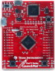
TM4C123G MCU
| I/O | Analog Function |
Digital Function (GPIOx->PCTL PMCn Field Encoding) | |||||||||||||||
| 0x0 | 0x1 | 0x2 | 0x3 | 0x4 | 0x5 | 0x6 | 0x7 | 0x8 | 0x9 | 0xA | 0xB | 0xC | 0xD | 0xE | 0xF | ||
| 0000 | 0001 | 0010 | 0011 | 0100 | 0101 | 0110 | 0111 | 1000 | 1001 | 1010 | 1011 | 1100 | 1101 | 1110 | 1111 | ||
| PA0 | — | GPIO | U0Rx | — | — | — | — | — | — | CAN1Rx | — | — | — | — | — | — | — |
| PA1 | — | GPIO | U0Tx | — | — | — | — | — | — | CAN1Tx | — | — | — | — | — | — | — |
| PA2 | — | GPIO | — | SSI0CLK | — | — | — | — | — | — | — | — | — | — | — | — | — |
| PA3 | — | GPIO | — | SSI0Fss | — | — | — | — | — | — | — | — | — | — | — | — | — |
| PA4 | — | GPIO | — | SSI0Rx | — | — | — | — | — | — | — | — | — | — | — | — | — |
| PA5 | — | GPIO | — | SSI0Tx | — | — | — | — | — | — | — | — | — | — | — | — | — |
| PA6 | — | GPIO | — | — | I2C1SCL | — | M1PWM2 | — | — | — | — | — | — | — | — | — | — |
| PA7 | — | GPIO | — | — | I2C1SDA | — | M1PWM3 | — | — | — | — | — | — | — | — | — | — |
| PB0 | USB0ID | GPIO | U1Rx | — | — | — | — | — | T2CCP0 | — | — | — | — | — | — | — | — |
| PB1 | USB0VBUS | GPIO | U1Tx | — | — | — | — | — | T2CCP1 | — | — | — | — | — | — | — | — |
| PB2 | — | GPIO | — | — | I2C0SCL | — | — | — | T3CCP0 | — | — | — | — | — | — | — | — |
| PB3 | — | GPIO | — | — | I2C0SDA | — | — | — | T3CCP1 | — | — | — | — | — | — | — | — |
| PB4 | AIN10 | GPIO | — | SSI2Clk | — | M0PWM2 | — | — | T1CCP0 | CAN0Rx | — | — | — | — | — | — | — |
| PB5 | AIN11 | GPIO | — | SSI2Fss | — | M0PWM3 | — | — | T1CCP1 | CAN0Tx | — | — | — | — | — | — | — |
| PB6 | — | GPIO | — | SSI2Rx | — | M0PWM0 | — | — | T0CCP0 | — | — | — | — | — | — | — | — |
| PB7 | — | GPIO | — | SSI2Tx | — | M0PWM1 | — | — | T0CCP1 | — | — | — | — | — | — | — | — |
| PC0 | — | GPIO | TCK SWCLK |
— | — | — | — | — | T4CCP0 | — | — | — | — | — | — | — | — |
| PC1 | — | GPIO | TMS SWDIO |
— | — | — | — | — | T4CCP1 | — | — | — | — | — | — | — | — |
| PC2 | — | GPIO | TDI | — | — | — | — | — | T5CCP0 | — | — | — | — | — | — | — | — |
| PC3 | — | GPIO | TDO SWO |
— | — | — | — | — | T5CCP1 | — | — | — | — | — | — | — | — |
| PC4 | C1- | GPIO | U4Rx | U1Rx | — | M0PWM6 | — | IDX1 | WT0CCP0 | U1RTS | — | — | — | — | — | — | — |
| PC5 | C1+ | GPIO | U4Tx | U1Tx | — | M0PWM7 | — | PhA1 | WT0CCP1 | U1CTS | — | — | — | — | — | — | — |
| PC6 | C0+ | GPIO | U3Rx | — | — | — | — | PhB1 | WT1CCP0 | USB0EPEN | — | — | — | — | — | — | — |
| PC7 | C0- | GPIO | U3Tx | — | — | — | — | — | WT1CCP1 | USB0PFLT | — | — | — | — | — | — | — |
| PD0 | AIN7 | GPIO | SSI3Clk | SSI1Clk | I2C3SCL | M0PWM6 | M1PWM0 | — | WT2CCP0 | — | — | — | — | — | — | — | — |
| PD1 | AIN6 | GPIO | SSI3Fss | SSI1Fss | I2C3SDA | M0PWM7 | M1PWM1 | — | WT2CCP1 | — | — | — | — | — | — | — | — |
| PD2 | AIN5 | GPIO | SSI3Rx | SSI1Rx | — | M0FAILT0 | — | — | WT3CCP0 | USB0EPEN | — | — | — | — | — | — | — |
| PD3 | AIN4 | GPIO | SSI3Tx | SSI1Tx | — | — | — | IDX0 | WT3CCP1 | USB0PFLT | — | — | — | — | — | — | — |
| PD4 | USB0DM | GPIO | U6Rx | — | — | — | — | — | WT4CCP0 | — | — | — | — | — | — | — | — |
| PD5 | USB0DP | GPIO | U6Tx | — | — | — | — | — | WT4CCP1 | — | — | — | — | — | — | — | — |
| PD6 | — | GPIO | U2Rx | — | — | M0FAULT0 | — | PhA0 | WT5CCP0 | — | — | — | — | — | — | — | — |
| PD7 | — | GPIO | U2Tx | — | — | — | — | PhB0 | WT5CCP1 | NMI | — | — | — | — | — | — | — |
| PE0 | AIN3 | GPIO | U7Rx | — | — | — | — | — | — | — | — | — | — | — | — | — | — |
| PE1 | AIN2 | GPIO | U7Tx | — | — | — | — | — | — | — | — | — | — | — | — | — | — |
| PE2 | AIN1 | GPIO | — | — | — | — | — | — | — | — | — | — | — | — | — | — | — |
| PE3 | AIN0 | GPIO | — | — | — | — | — | — | — | — | — | — | — | — | — | — | — |
| PE4 | AIN9 | GPIO | U5Rx | — | I2C2SCL | M0PWM4 | M1PWM2 | — | — | CAN0Rx | — | — | — | — | — | — | — |
| PE5 | AIN8 | GPIO | U5Tx | — | I2C3SDA | M0PWM5 | M1PWM3 | — | — | CAN0TX | — | — | — | — | — | — | — |
| PF0 | — | GPIO | U1RTS | SSI1Rx | CAN0Rx | — | M1PWM4 | PhA0 | T0CCP0 | NMI | C0o | — | — | — | — | — | — |
| PF1 | — | GPIO | U1CTS | SSI1Tx | — | — | M1PWM5 | PhB0 | T0CCP1 | — | C1o | — | — | — | — | TRD1 | — |
| PF2 | — | GPIO | — | SSI1Clk | — | M0FAULT0 | M1PWM6 | — | T1CCP0 | — | — | — | — | — | — | TRD0 | — |
| PF3 | — | GPIO | — | SSI1Fss | CAN0Tx | — | M1PWM7 | — | T1CCP1 | — | — | — | — | — | — | TRCLK | — |
| PF4 | — | GPIO | — | — | — | — | M1FAULT0 | IDX0 | T2CCP0 | USB0EPEN | — | — | — | — | — | — | — |
| I/O | Analog Function |
0000 | 0001 | 0010 | 0011 | 0100 | 0101 | 0110 | 0111 | 1000 | 1001 | 1010 | 1011 | 1100 | 1101 | 1110 | 1111 |
| 0x0 | 0x1 | 0x2 | 0x3 | 0x4 | 0x5 | 0x6 | 0x7 | 0x8 | 0x9 | 0xA | 0xB | 0xC | 0xD | 0xE | 0xF | ||
| Digital Function (GPIOx->PCTL PMCn Field Encoding) | |||||||||||||||||
PD7 and PF0 are configured as GPIO by default but is locked and can only be reprogrammed by unlocking the pin in the GPIOLOCK register and uncommitting it by setting the GPIOCR register.
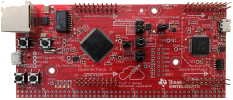
TM4C1294 MCU
| I/O | Analog Function |
Digital Function (GPIOx->PCTL PMCn Field Encoding) | |||||||||||||||
| 0x0 | 0x1 | 0x2 | 0x3 | 0x4 | 0x5 | 0x6 | 0x7 | 0x8 | 0x9 | 0xA | 0xB | 0xC | 0xD | 0xE | 0xF | ||
| 0000 | 0001 | 0010 | 0011 | 0100 | 0101 | 0110 | 0111 | 1000 | 1001 | 1010 | 1011 | 1100 | 1101 | 1110 | 1111 | ||
| PA0 | — | GPIO | U0Rx | I2C9SCL | T0CCP0 | — | — | — | CAN0Rx | — | — | — | — | — | — | — | — |
| PA1 | — | GPIO | U0Tx | I2C9SDA | T0CCP1 | — | — | — | CAN0Tx | — | — | — | — | — | — | — | — |
| PA2 | — | GPIO | U4Rx | I2C8SCL | T1CCP0 | — | — | — | — | — | — | — | — | — | — | — | SSI0CLK |
| PA3 | — | GPIO | U4Tx | I2C8SDA | T1CCP1 | — | — | — | — | — | — | — | — | — | — | — | SSI0Fss |
| PA4 | — | GPIO | U3Rx | I2C7SCL | T2CCP0 | — | — | — | — | — | — | — | — | — | — | — | SSI0XDAT0 |
| PA5 | — | GPIO | U3Tx | I2C7SDA | T2CCP1 | — | — | — | — | — | — | — | — | — | — | — | SSI0XDAT1 |
| PA6 | — | GPIO | U2Rx | I2C6SCL | T3CCP0 | — | USB0EPEN | — | — | — | — | — | — | — | SSI0XDAT2 | — | EPI0S8 |
| PA7 | — | GPIO | U2Tx | I2C6SDA | T3CCP1 | — | USB0PFLT | — | — | — | — | — | USB0EPEN | — | SSI0XDA3 | — | EPI0S9 |
| PB0 | USB0ID | GPIO | U1Rx | I2C5SCL | T4CCP0 | — | — | — | CAN1Rx | — | — | — | — | — | — | — | — |
| PB1 | USB0VBUS | GPIO | U1Tx | I2C5SDA | T4CCP1 | — | — | — | CAN1Tx | — | — | — | — | — | — | — | — |
| PB2 | — | GPIO | — | I2C0SCL | T5CCP0 | — | — | — | — | — | — | — | — | — | — | USB0STP | EPI0S27 |
| PB3 | — | GPIO | — | I2C0SDA | T5CCP1 | — | — | — | — | — | — | — | — | — | — | USB0CLK | EPI0S28 |
| PB4 | AIN10 | GPIO | U0CTS | I2C5SCL | — | — | — | — | — | — | — | — | — | — | — | — | SSI1Fss |
| PB5 | AIN11 | GPIO | U0RTS | I2C5SDA | — | — | — | — | — | — | — | — | — | — | — | — | SSI1Clk |
| PC0 | — | GPIO | TCK SWCLK |
— | — | — | — | — | — | — | — | — | — | — | — | — | — |
| PC1 | — | GPIO | TMS SWDIO |
— | — | — | — | — | — | — | — | — | — | — | — | — | — |
| PC2 | — | GPIO | TDI | — | — | — | — | — | — | — | — | — | — | — | — | — | — |
| PC3 | — | GPIO | TDO SWO |
— | — | — | — | — | — | — | — | — | — | — | — | — | — |
| PC4 | C1- | GPIO | U7Rx | — | — | — | — | — | — | — | — | — | — | — | — | — | EPI0S7 |
| PC5 | C1+ | GPIO | U7Tx | — | — | — | — | — | RTCCLK | — | — | — | — | — | — | — | EPI0S6 |
| PC6 | C0+ | GPIO | U5Rx | — | — | — | — | — | — | — | — | — | — | — | — | — | EPI0S5 |
| PC7 | C0- | GPIO | U5Tx | — | — | — | — | — | — | — | — | — | — | — | — | — | EPI0S4 |
| PD0 | AIN15 | GPIO | — | I2C7SCL | T0CCP0 | — | C0o | — | — | — | — | — | — | — | — | — | SSI2XDAT1 |
| PD1 | AIN14 | GPIO | — | I2C7SDA | T0CCP1 | — | C1o | — | — | — | — | — | — | — | — | — | SSI2XDAT0 |
| PD2 | AIN13 | GPIO | — | I2C8SCL | T1CCP0 | — | C2o | — | — | — | — | — | — | — | — | — | SSI2Fass |
| PD3 | AIN12 | GPIO | — | I2C8SDA | T1CCP1 | — | — | — | — | — | — | — | — | — | — | — | SSI2Clk |
| PD4 | AIN7 | GPIO | U2Rx | — | T3CCP0 | — | — | — | — | — | — | — | — | — | — | — | SSI1XDAT2 |
| PD5 | AIN6 | GPIO | U2Tx | — | T3CCP1 | — | — | — | — | — | — | — | — | — | — | — | SSI1XDAT3 |
| PD6 | AIN5 | GPIO | U2RTS | — | T4CCP0 | — | USB0EPEN | — | — | — | — | — | — | — | — | — | SSI2XDAT3 |
| PD7 | AIN4 | GPIO | U2CTS | — | T4CCP1 | — | USB0OFLT | — | — | NMI | — | — | — | — | — | — | SSI2XDAT2 |
| PE0 | AIN3 | GPIO | U1RTS | — | — | — | — | — | — | — | — | — | — | — | — | — | — |
| PE1 | AIN2 | GPIO | U1DSR | — | — | — | — | — | — | — | — | — | — | — | — | — | — |
| PE2 | AIN1 | GPIO | U1DCD | — | — | — | — | — | — | — | — | — | — | — | — | — | — |
| PE3 | AIN0 | GPIO | U1DTR | — | — | — | — | — | — | — | — | — | — | — | — | — | — |
| PE4 | AIN9 | GPIO | U1RI | — | — | — | — | — | — | — | — | — | — | — | — | — | SSI1XDAT0 |
| PE5 | AIN8 | GPIO | — | — | — | — | — | — | — | — | — | — | — | — | — | — | SSIXDAT1 |
| PF0 | — | GPIO | — | — | — | — | EN0LED0 | M0PWM0 | — | — | — | — | — | — | — | SSI3XDAT1 | TRD2 |
| PF1 | — | GPIO | — | — | — | — | EN0LED2 | M0PWM1 | — | — | — | — | — | — | — | SSI3XDAT0 | TRD1 |
| PF2 | — | GPIO | — | — | — | — | — | M0PWM2 | — | — | — | — | — | — | — | SSI3Fss | TRD0 |
| PF3 | — | GPIO | — | — | — | — | — | M0PWM3 | — | — | — | — | — | — | — | SSI3Clk | TRCLK |
| PF4 | — | GPIO | — | — | — | — | EN0LED1 | M0FAULT0 | — | — | — | — | — | — | — | SSI3XDA2 | TRD3 |
| IO | Analog Function | Digital Function (GPIOx->PCTL PMCn Field Encoding) | |||||||||||||||
| 0x0 | 0x1 | 0x2 | 0x3 | 0x4 | 0x5 | 0x6 | 0x7 | 0x8 | 0x9 | 0xA | 0xB | 0xC | 0xD | 0xE | 0xF | ||
| 0000 | 0001 | 0010 | 0011 | 0100 | 0101 | 0110 | 0111 | 1000 | 1001 | 1010 | 1011 | 1100 | 1101 | 1110 | 1111 | ||
| PG0 | — | GPIO | — | I2C1SLC | — | — | EN0PPS | M0PWM4 | — | — | — | — | — | — | — | — | EPI0S11 |
| PG1 | — | GPIO | — | I2C1SDA | — | — | — | M0PWM5 | — | — | — | — | — | — | — | — | EPI0S10 |
| PH0 | — | GPIO | U0RTS | — | — | — | — | — | — | — | — | — | — | — | — | — | EPI0S0 |
| PH1 | — | GPIO | U0CTS | — | — | — | — | — | — | — | — | — | — | — | — | — | EPI0S1 |
| PH2 | — | GPIO | U0DCD | — | — | — | — | — | — | — | — | — | — | — | — | — | EPI0S2 |
| PH3 | — | GPIO | U0DSR | — | — | — | — | — | — | — | — | — | — | — | — | — | EPI0S3 |
| PJ0 | — | GPIO | U3Rx | — | — | — | EN0PPS | — | — | — | — | — | — | — | — | — | — |
| PJ1 | — | GPIO | U3Tx | — | — | — | — | — | — | — | — | — | — | — | — | — | — |
| PK0 | AIN16 | GPIO | U4Rx | — | — | — | — | — | — | — | — | — | — | — | — | — | EPI0S0 |
| PK1 | AIN17 | GPIO | U4Tx | — | — | — | — | — | — | — | — | — | — | — | — | — | EPI0S1 |
| PK2 | AIN18 | GPIO | U4RTS | — | — | — | — | — | — | — | — | — | — | — | — | — | EPI0S2 |
| PK3 | AIN19 | GPIO | U4CTS | — | — | — | — | — | — | — | — | — | — | — | — | — | EPI0S3 |
| PK4 | — | GPIO | — | I2C3SCL | — | — | EN0LED0 | M0PWM6 | — | — | — | — | — | — | — | — | EPI0S32 |
| PK5 | — | GPIO | — | I2C3SDA | — | — | EN0LED2 | M0PWM7 | — | — | — | — | — | — | — | — | EPI0S31 |
| PK6 | — | GPIO | — | I2C4SCL | — | — | EN0LED1 | M0FAULT1 | — | — | — | — | — | — | — | — | EPI0S25 |
| PK7 | — | GPIO | U0RI | I2C4SDA | — | — | RTCCLK | M0FAULT2 | — | — | — | — | — | — | — | — | EPI0S24 |
| PL0 | — | GPIO | — | I2C2SDA | — | — | — | M0FAULT3 | — | — | — | — | — | — | — | USB0D0 | EPI0S16 |
| PL1 | — | GPIO | — | I2C2SCL | — | — | — | PhA0 | — | — | — | — | — | — | — | USB0D1 | EPI0S17 |
| PL2 | — | GPIO | — | — | — | — | C0o | PhB0 | — | — | — | — | — | — | — | USB0D2 | EPI0S18 |
| PL3 | — | GPIO | — | — | — | — | C1o | IDX0 | — | — | — | — | — | — | — | USB0D3 | EPI0S19 |
| PL4 | — | GPIO | — | — | T0CCP0 | — | — | — | — | — | — | — | — | — | — | USB0D4 | EPI0S26 |
| PL5 | — | GPIO | — | — | T0CCP1 | — | — | — | — | — | — | — | — | — | — | USB0D5 | EPI0S33 |
| PL6 | USB0DP | GPIO | — | — | T1CCP0 | — | — | — | — | — | — | — | — | — | — | — | — |
| PL7 | USB0DM | GPIO | — | — | T1CCP1 | — | — | — | — | — | — | — | — | — | — | — | — |
| PM0 | — | GPIO | — | — | T2CCP0 | — | — | — | — | — | — | — | — | — | — | — | EPI0S15 |
| PM1 | — | GPIO | — | — | T2CCP1 | — | — | — | — | — | — | — | — | — | — | — | EPI0S14 |
| PM2 | — | GPIO | — | — | T3CCP0 | — | — | — | — | — | — | — | — | — | — | — | EPI0S13 |
| PM3 | — | GPIO | — | — | T3CCP1 | — | — | — | — | — | — | — | — | — | — | — | EPI0S12 |
| PM4 | TMPR3 | GPIO | U0CTS | — | T4CCP0 | — | — | — | — | — | — | — | — | — | — | — | — |
| PM5 | TMPR2 | GPIO | U0DCD | — | T4CCP1 | — | — | — | — | — | — | — | — | — | — | — | — |
| PM6 | TMPR1 | GPIO | U0DSR | — | T5CCP0 | — | — | — | — | — | — | — | — | — | — | — | — |
| PM7 | TMPR0 | GPIO | U0RI | — | T5CCP1 | — | — | — | — | — | — | — | — | — | — | — | — |
| PN0 | — | GPIO | U1RTS | — | — | — | — | — | — | — | — | — | — | — | — | — | — |
| PN1 | — | GPIO | U1CTS | — | — | — | — | — | — | — | — | — | — | — | — | — | — |
| PN2 | — | GPIO | U1DCD | U2RTS | — | — | — | — | — | — | — | — | — | — | — | — | EPI0S29 |
| PN3 | — | GPIO | U1DSR | U2CTS | — | — | — | — | — | — | — | — | — | — | — | — | EPI0S30 |
| PN4 | — | GPIO | U1DTR | U3RTS | I2C2SDA | — | — | — | — | — | — | — | — | — | — | — | EPI0S34 |
| PN5 | — | GPIO | U1RI | U3CTS | I2C2SCL | — | — | — | — | — | — | — | — | — | — | — | EPI0S35 |
| PP0 | C2+ | GPIO | U6Rx | — | — | — | — | — | — | — | — | — | — | — | — | — | SSI3XDAT2 |
| PP1 | C2- | GPIO | U6Tx | — | — | — | — | — | — | — | — | — | — | — | — | — | SSI3XDAT3 |
| PP2 | — | GPIO | U0DTR | — | — | — | — | — | — | — | — | — | — | — | — | USB0NXT | EPI0S29 |
| PP3 | — | GPIO | U1CTS | U0DCD | — | — | — | — | RTCCLK | — | — | — | — | — | — | USB0DIR | EPI0S30 |
| PP4 | — | GPIO | U3RTS | U0DSR | — | — | — | — | — | — | — | — | — | — | — | USB0D7 | — |
| PP5 | — | GPIO | U3CTS | I2C2SCL | — | — | — | — | — | — | — | — | — | — | — | USB0D6 | — |
| PQ0 | — | GPIO | — | — | — | — | — | — | — | — | — | — | — | — | — | SSI3Clk | EPI0S20 |
| PQ1 | — | GPIO | — | — | — | — | — | — | — | — | — | — | — | — | — | SSI3Fss | EPI0S21 |
| PQ2 | — | GPIO | — | — | — | — | — | — | — | — | — | — | — | — | — | SSI3XDAT0 | EPI0S22 |
| PQ3 | — | GPIO | — | — | — | — | — | — | — | — | — | — | — | — | — | SSI3XDAT1 | EPI0S23 |
| PQ4 | — | GPIO | U1Rx | — | — | — | — | — | DIVSCLK | — | — | — | — | — | — | — | — |
| I/O | Analog Function |
0000 | 0001 | 0010 | 0011 | 0100 | 0101 | 0110 | 0111 | 1000 | 1001 | 1010 | 1011 | 1100 | 1101 | 1110 | 1111 |
| 0x0 | 0x1 | 0x2 | 0x3 | 0x4 | 0x5 | 0x6 | 0x7 | 0x8 | 0x9 | 0xA | 0xB | 0xC | 0xD | 0xE | 0xF | ||
| Digital Function (GPIOx->PCTL PMCn Field Encoding) | |||||||||||||||||
PD7 and PE7 are configured as GPIO by default but is locked and can only be reprogrammed by unlocking the pin in the GPIOLOCK register and uncommitting it by setting the GPIOCR register.