
Lesson 09: GPIO Ports and Configurations
The microprocessors access their I/O (Input/Output) devices either via special I/O instructions that read and write to peripherals located in a separate I/O address space, called "Port Mapped I/O, PMIO", or via instructions that access memory, called "Memory-mapped I/O, MMIO". ARM-based processors use memory-mapped I/O. The I/O ports share the same address space as memory. That means the software can access an I/O port simply by reading from or writing to the appropriate address, and these addresses are usually called "Registers". Most I/O ports can be configured for different I/O functions via registers; you can find detailed information about I/O registers in the microprocessor's datasheet.
Even though the accessing I/O register looks like reads and writes to memory variables, there are still some differences between the memory and I/O Registers. For example, some bits in the Register are read-only, and some are write-only; some bits can only be cleared or set; some bits cannot be modified, and some are reserved for future use.
General-Purpose Input/Output (GPIO)
A GPIO is a generic pin on a microcontroller that can be controlled by the program at runtime. GPIO pins have no predefined purpose and can be operated as parallel interfaces. It allows the microcontroller to exchange digital information with external devices. For example, GPIO can be used to read from a temperature sensor and to write to an LCD module or LEDs for status.
GPIO pins have the following capabilities:
- GPIO pins can be configured to be input or output
- GPIO pins can be enabled or disabled
- Input values are readable( typically logic high or low)
- Output values are writable and can be read back
- The input pin can be used to trigger the interrupt function
Instead of directly configuring and controlling each individual GPIO pin, we set up a group of GPIO pins (typically 8 GPIO pins) into a PORT. Through the PORT registers, we can simultaneously control and access multiple GPIO pins.
9.1 Texas Instruments Tiva TM4C I/O Ports
Texas Instruments Tiva TM4C I/O Ports
GPIO Ports
The general-purpose I/O pins on a TM4C device are grouped into ports. Each port is up to 8 bits wide (pins 0 ~ 7), has its own block of configuration registers, and is named by a letter (Port A, Port B, …). The two microcontrollers used in this course differ significantly in the number of ports they have and the functions those ports support, so we look at each one separately.
EK-TM4C123GXL LaunchPad
GPIO Ports
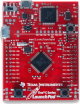
The microcontroller on the EK-TM4C123GXL LaunchPad is TM4C123GH6PM. The TM4C123GH6PM GPIO module comprises six physical GPIO blocks, each corresponding to an individual GPIO port (Port A, Port B, Port C, Port D, Port E, and Port F).
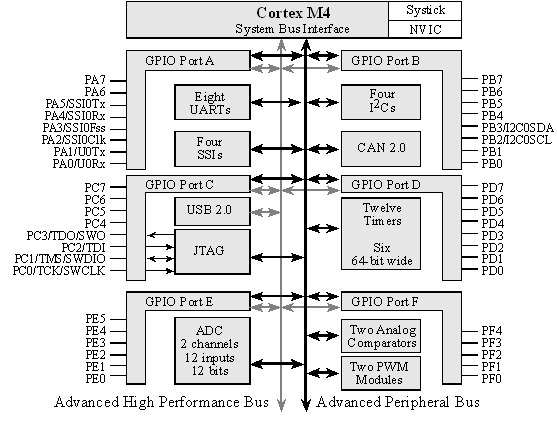
Figure 1: I/O Port Pins for the TM4C123GH6PM (From http://users.ece.utexas.edu/~valvano/Volume1/E-Book/C6_MicrocontrollerPorts.htm)
Port A ~ Port D have 8-pin I/O on each port; Port E has 6 pins, and Port F has 5 pins.
On the TM4C123G LaunchPad, all GPIO inputs are 5V-tolerant, except for a few GPIOs (PB0, PB1, and PD5). The 5V-tolerant feature of Tiva C MCUs enables us to use legacy external interfaces and devices, such as sensors, external modules, and legacy microcontrollers, without requiring additional logic-level translator circuits. Although most pins are 5V-tolerant, that doesn't necessarily mean the logic level is 5V TTL. The logic level voltage limits are still defined with respect to VDD, which is 3.3V.
On the TM4C123G microcontrollers, the GPIO Ports can be connected to either the Advanced Peripheral Bus (APB) or the Advanced High-performance Bus (AHB). After reset, the GPIO Ports are connected to the legacy APB bus and through the APB memory aperture. Each GPIO port can be individually configured to use AHB or APB through the "Register 9: GPIO High-Performance Bus Control (GPIOHBCTL), offset 0x06C". The AHB bus offers superior back-to-back access performance compared to the APB bus.
Table 1: GPIO Ports' Base Address
| APB Bus | AHB Bus | |||
| GPIO Port | Base Address | Range | Base Address | Range |
| Port A | 0x4000.4000 | 0x4000.4000 ~ 0x4000.4FFF | 0x4005.8000 | 0x4005.8000 ~ 0x4005.8FFF |
| Port B | 0x4000.5000 | 0x4000.5000 ~ 0x4000.5FFF | 0x4005.9000 | 0x4005.9000 ~ 0x4005.9FFF |
| Port C | 0x4000.6000 | 0x4000.6000 ~ 0x4000.6FFF | 0x4005.A000 | 0x4005.A000 ~ 0x4005.AFFF |
| Port D | 0x4000.7000 | 0x4000.7000 ~ 0x4000.7FFF | 0x4005.B000 | 0x4005.B000 ~ 0x4005.BFFF |
| Port E | 0x4002.4000 | 0x4002.4000 ~ 0x4002.4FFF | 0x4005.C000 | 0x4005.C000 ~ 0x4005.CFFF |
| Port F | 0x4002.5000 | 0x4002.5000 ~ 0x4002.5FFF | 0x4005.D000 | 0x4005.D000 ~ 0x4005.DFFF |
Each GPIO port has 4KB of memory space because it has many special-function registers. The GPIO Data Register supports bit-specific addressing, allowing a single instruction to access data ranging from 1 bit to 8 bits in the memory map.
The TM4C123GH6PM provides 43 GPIO pins across six ports (Port A ~ Port F). On this course, all six ports stay on the legacy APB aperture after reset, so the plain GPIOx names are used throughout (no _AHB suffix).
Table 1: TM4C123GH6PM GPIO Ports Summary
| Port | Pins | Width | Notes |
|---|---|---|---|
| Port A | PA0~PA7 | 8 | |
| Port B | PB0~PB7 | 8 | PB0, PB1 are not 5V-tolerant |
| Port C | PC0~PC7 | 8 | PC0~PC3 = JTAG/SWD (protected) |
| Port D | PD0~PD7 | 8 | PD7 = NMI (protected); PD5 is not 5V-tolerant |
| Port E | PE0~PE5 | 6 | |
| Port F | PF0~PF4 | 5 | PF0 = NMI (protected); LaunchPad LEDs on PF1~PF3, switches on PF0/PF4 |
On the EK-TM4C123GXL LaunchPad: Red = PF1, Blue = PF2, Green = PF3; SW1 = PF4, SW2 = PF0.
Registers
| Address | bit-Field | GPIO Register Name | ||||||||
| 7 | 6 | 5 | 4 | 3 | 2 | 1 | 0 | In Assembly | In C | |
| $400F.E108 | -- | -- | GPIOF | GPIOE | GPIOD | GPIOC | GPIOB | GPIOA | SYSCTL_RCGCGPIO_R | SYSCTL->RCGCGPIO |= (_PORTs); |
| PORTn BaseAddr + $3FC | DATA | DATA | DATA | DATA | DATA | DATA | DATA | DATA | GPIO_PORTn_DATA_R | GPIOn->DATA |
| PORTn BaseAddr + $400 | DIR | DIR | DIR | DIR | DIR | DIR | DIR | DIR | GPIO_PORTn_DIR_R | GPIOn->DIR |
| PORTn BaseAddr + $420 | SEL | SEL | SEL | SEL | SEL | SEL | SEL | SEL | GPIO_PORTn_AFSEL_R | GPIOn->AFSEL |
| PORTn BaseAddr + $50C | ODR | ODR | ODR | ODR | ODR | ODR | ODR | GPIO_PORTn_ODR_R | GPIOn->ODR | |
| PORTn BaseAddr + $510 | PUE | PUE | PUE | PUE | PUE | PUE | PUE | PUE | GPIO_PORTn_PUR_R | GPIOn->PUR |
| PORTn BaseAddr + $514 | PDE | PDE | PDE | PDE | PDE | PDE | PDE | PDE | GPIO_PORTn_PDR_R | GPIOn->PDR |
| PORTn BaseAddr + $51C | DEN | DEN | DEN | DEN | DEN | DEN | DEN | DEN | GPIO_PORTn_DEN_R | GPIOn->DEN |
| PORTn BaseAddr + $524 | 1 | 1 | 1 | 1 | 1 | 1 | 1 | 1 | GPIO_PORTn_CR_R | GPIOn->CR |
| PORTn BaseAddr + $528 | 0 | 0 | 0 | 0 | 0 | 0 | 0 | 0 | GPIO_PORTn_AMSEL_R | GPIOn->AMSEL |
| 31-28 | 27-24 | 23-20 | 19-16 | 15-12 | 11-8 | 7-4 | 3-0 | |||
| PORTn BaseAddr + $52C | PMC7 | PMC6 | PMC5 | PMC4 | PMC3 | PMC2 | PMC1 | PMC0 | GPIO_PORTn_PCTL_R | GPIOn->PCTL |
| PORTC BaseAddr + $520 | LOCK (write 0x4C4F434B to unlock, other locks) (reads 1 if locked, 0 if unlocked) | GPIO_PORTC_LOCK_R | GPIOC->LOCK | |||||||
| PORTD BaseAddr + $520 | LOCK (write 0x4C4F434B to unlock, other locks) (reads 1 if locked, 0 if unlocked) | GPIO_PORTD_LOCK_R | GPIOD->LOCK | |||||||
| PORTF BaseAddr + $520 | LOCK (write 0x4C4F434B to unlock, other locks) (reads 1 if locked, 0 if unlocked) | GPIO_PORTF_LOCK_R | GPIOF->LOCK | |||||||
* GPIOn ➤ GPIOA, GPIOB, GPIOC, GPIOD, GPIOE, and GPIOF
On-board I/O
- Two USB connectors on the board.
- The top one is an integrated In-Circuit Debug Interface (ICDI), which allows programming and debugging of the onboard TM4C microcontroller.
- The left USB connector enables you to develop USB applications (either as a device or a host).
- Switch-selectable power sources
Select one of the two power sources
- Left-Hand DEVICE Position: powered by USB device port
- Right-Hand DEBUG Position: powered by USB debug (ICDI) port
- Reset button
- Two user switches (SW1 and SW2)
- RGB User LED
- Stackable 40-pin BoosterPack XL interface
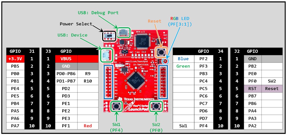
Figure 2: Pinout for the TM4C123GXL LaunchPad
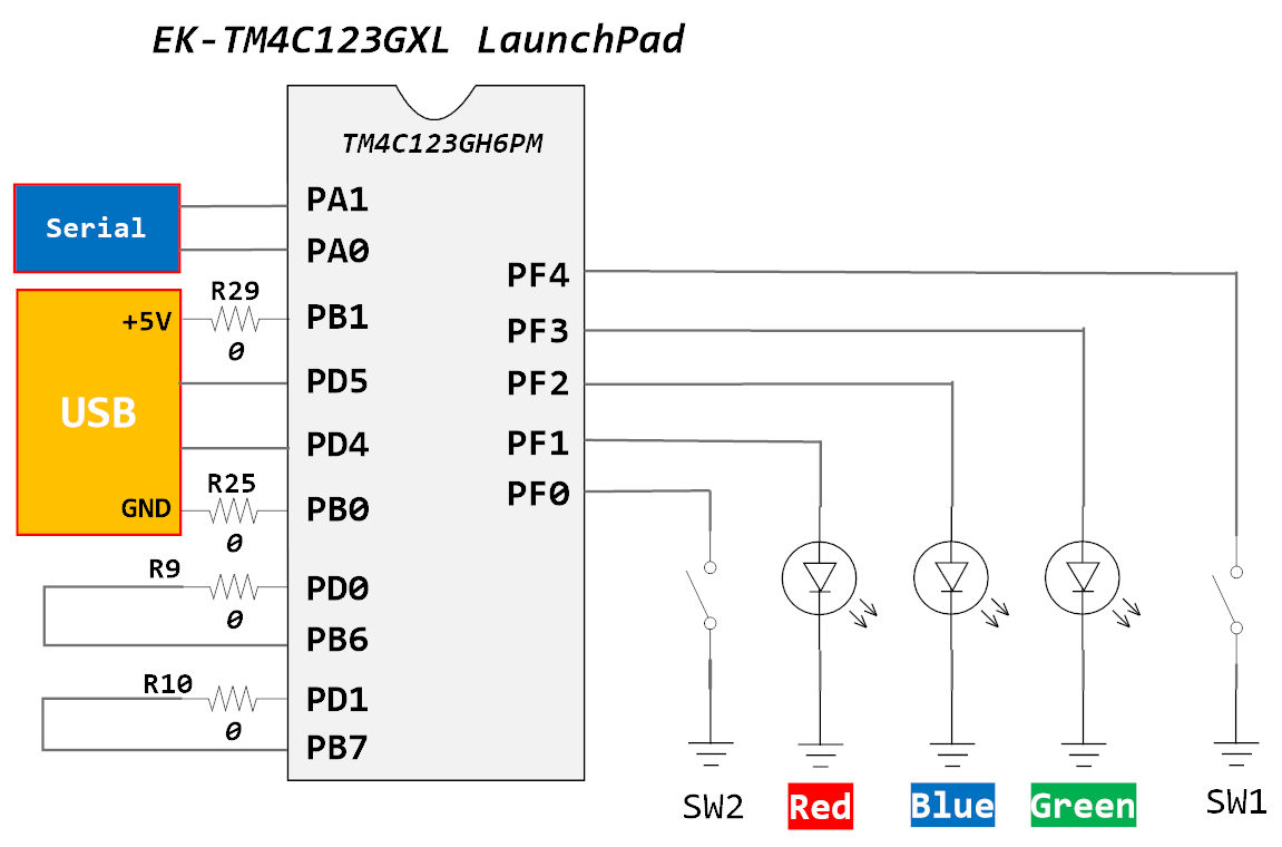
Figure 3: User Switches and RGB LED Signals
Sample Firmware Code in Assembly
Launch Keil μVision5 on your computer, then create a new project. Copy and paste the following source code into your main.s
Please download the definition ZIP file and extract it into the same project folder: TM4C123GH6PM.zip
The following source code is to turn on the onboard switches and RGB LEDs on PORTF
;This is the first ARM Assembly language program you see in the lab
;This program template was created by Airs Lin @ 2017 California State University of Los Angeles.
;When you write your program, you could have your info at the top document block
;For Example:  Your Name, Student Number, what the program is for, and what it does etc.

            INCLUDE     TM4C123GH6PM.s

; Constant Variable Here
STACK_ADDR_123G     EQU     0x20008000
LED_R               EQU     2_00000010
LED_B               EQU     2_00000100
LED_G               EQU     2_00001000
SW1                 EQU     2_00010000
SW2                 EQU     2_00000001

            THUMB

; Vector Table Mapped to Address 0 at Reset
; Linker requires __Vectors to be exported

            AREA    RESET, DATA, READONLY
            EXPORT  __Vectors
__Vectors
            DCD     STACK_ADDR_123G         ; stack pointer value when stack is empty
            DCD     Reset_Handler           ; reset vector

            ALIGN

; The program
; Linker requires Reset_Handler

            AREA    |.text|, CODE, READONLY
            ENTRY                           ; mark first instruction to execute
            EXPORT  Reset_Handler
Reset_Handler
; This subroutine grants access to
; floating point coprocessor.
; It is called by the startup code.
            LDR     R0, =0xE000ED88
                    ; Enable CP10,CP11
            LDR     R1,[R0]
            ORR     R1,R1,#0x20
            STR     R1,[R0]
            DSB                             ; wait for store to complete
            ISB                             ;reset pipeline now the FPU is enabled

;=====================
; 1. Turn on Port F clock in SYSCTL_RCGCGPIO_R, then chcek SYSCTL_PRGPIO_R ready flag
; enable clock to GPIOF at clock gating register
            LDR     R0, =SYSCTL_RCGCGPIO_R  ; RCGC reg. addr.
            LDR     R1, [R0]
            ORR     R1, #(GPIO_PORTF)
            STR     R1, [R0]

            LDR     R0, =SYSCTL_PRGPIO_R
WAIT4GPIO   LDR     R1, [R0]
            TST     R1, #(GPIO_PORTF)
            BEQ     WAIT4GPIO

; 2. Unlock PF0 and/or PD7 for TM4C123G board
; unlock PortF
            LDR     R0, =PORT_UNLOCK_CODE
            LDR     R1, [R0]
            LDR     R0, =GPIO_PORTF_LOCK_R
            STR     R1, [R0]
            NOP
            NOP

            LDR     R0, =GPIO_PORTF_CR_R    ; Enable Commit for PF0
            LDR     R1, [R0]
            ORR     R1, #0x01
            STR     R1, [R0]
; 3. Clear AMSEL to disable analog
            LDR     R0, =GPIO_PORTF_AMSEL_R
            MOV     R1, #0x00
            STR     R1, [R0]
; 4. Clear PCTL to select GPIO
            LDR     R0, =GPIO_PORTF_PCTL_R
            MOV     R1, #0x0000
            STR     R1, [R0]
; 5. Clear AFSEL bits to 0 to select regular I/O
            LDR     R0, = GPIO_PORTF_AFSEL_R
            MOV     R1, #0x00
            STR     R1, [R0]
; 6. Set DIR to 0 for input, 1 for output
; set PORTF pin3-1 as output pins
            LDR     R0, =GPIO_PORTF_DIR_R
            MOV     R1, #0x0E               ; pin 1, 2 and 3 are output
            STR     R1, [R0]
; 7. Set PUR bits to 1 to enable internal pull-up
            LDR     R0, =GPIO_PORTF_PUR_R
            MOV     R1, #0x11               ; pin 0 and 4 connect with switch
            STR     R1, [R0]
; 8 Set DEN bits to 1 to enable data pins
            LDR     R0, =GPIO_PORTF_DEN_R
            LDR     R1, [R0]
            ORR     R1, #0x1F
            STR     R1, [R0]

;;;;;;;;;; Your Main Code Starts from the next line ;;;;;;;;;;;;


DeadLoop    B       DeadLoop                ; Infinite loop to end program

; The constant variable area
; The value will be stored on ROM segment
            AREA    ConstantVariables, DATA, READONLY
PORT_UNLOCK_CODE    DCD 0x4C4F434B


; The variables area
; The variables will be assigned to RAM area
            AREA    Variables, DATA, READWRITE

            END     ; End of the program
Keil C Sample Firmware Code
The following source code is to turn on the onboard RGB LEDs and switch button (SW2) on PORTF
#include <stdio.h>
#include <stdlib.h>
#include <stdint.h>
#include <stdbool.h>

#include "TM4C123GH6PM.h"

void Setup_GPIO();
void DelayMs(int s);

int main(void)
{
    Setup_GPIO();

    while(1){
        if ( GPIOF->DATA & 0x01 ){
            GPIOF->DATA = 0x02;
            DelayMs(1000);
            GPIOF->DATA = 0x04;
            DelayMs(1000);
            GPIOF->DATA = 0x08;
            DelayMs(1000);
        } else {
            GPIOF->DATA = 0x0E;
            DelayMs(1000);
            GPIOF->DATA = 0x00;
            DelayMs(1000);
        }
    }
}
void Setup_GPIO()
{
    // GPIO Initialization and Configuration
    // 1. Enable Clock to the GPIO Modules (SYSCTL->RCGCGPIO |= (_PORTs);)
    SYSCTL->RCGCGPIO |= (_PORTs); |= 0x20;
    // allow time for clock to stabilize (SYSCTL->PRGPIO)
    while((SYSCTL->PRGPIO & (0x20) ) != (0x20) ){};
    // 2. Unlock GPIO only PD7, PF0 on TM4C123G; PD7, PE7 on TM4C1294 (GPIOx->LOCK = 0x4C4F434B; and GPIOx->CR = _PINs;)
    GPIOF->LOCK = 0x4C4F434B;
    GPIOF->CR |= 0x01;
    // 3. Set Analog Mode Select bits for each Port (GPIOn->AMSEL 0=digital, 1=analog)
    GPIOF->AMSEL = 0x00;
    // 4. Set Port Control Register for each Port (GPIOn->PCTL = PMCn, check the PCTL table)
    GPIOF->PCTL = 0x00;
    // 5. Set Alternate Function Select bits for each Port (GPIOn->AFSEL 0=regular I/O, 1=PCTL peripheral)
    GPIOF->AFSEL = 0x00;
    // 6. Set the output pins for each port only (Direction of the Pins: GPIOn->DIR 0=input, 1=output)
    GPIOF->DIR = 0x0E; // PF3,PF2,PF1 for Output
    // 7. Set PUR bits for internal pull-up, PDR for pull-down reg, ODR for open drain
    GPIOF->PUR = 0x01;
    // 8. Set Digital ENable register on all GPIO pins (GPIOn->DEN 0=disable, 1=enable)
    GPIOF->DEN = 0x0F; // Enable all digital pins on PortF (PF3,PF2,PF1,PF0)
}
void DelayMs(int s)
{
    volatile int i, j;
    for (i = 0; i < s; i++)
        for (j = 0; j < 3180; j++)
            {};
}
EK-TM4C1294XL LaunchPad
GPIO Ports
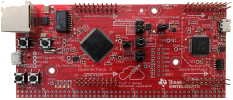
The microcontroller on the EK-TM4C1294XL LaunchPad is TM4C1294NCPDT. The TM4C1294NCPDT GPIO module comprises fifteen physical GPIO blocks, each corresponding to an individual GPIO port (Port A, Port B, Port C, Port D, Port E, Port F, Port G, Port H, Port J, Port K, Port L, Port M, Port N, Port P, and Port Q).
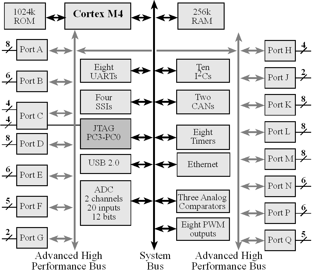
On the TM4C1294 microcontroller, the Advanced High-Performance Bus (AHB) is now the default connection for Port A ~ Q. The move from APB to AHB reduces clock latency, so you would get better performance with direct GPIO. The base addresses for each GPIO Port are shown in Table 2.
Table 2: GPIO Ports' Base Address
| AHB Bus | ||
| GPIO Port | Base Address | Range |
| Port A | 0x4005.8000 | 0x4005.8000 ~ 0x4005.8FFF |
| Port B | 0x4005.9000 | 0x4005.9000 ~ 0x4005.9FFF |
| Port C | 0x4005.A000 | 0x4005.A000 ~ 0x4005.AFFF |
| Port D | 0x4005.B000 | 0x4005.B000 ~ 0x4005.BFFF |
| Port E | 0x4005.C000 | 0x4005.C000 ~ 0x4005.CFFF |
| Port F | 0x4005.D000 | 0x4005.D000 ~ 0x4005.DFFF |
| Port G | 0x4005.E000 | 0x4005.E000 ~ 0x4005.EFFF |
| Port H | 0x4005.F000 | 0x4005.F000 ~ 0x4005.FFFF |
| Port J | 0x4006.0000 | 0x4006.0000 ~ 0x4006.0FFF |
| Port K | 0x4006.1000 | 0x4006.1000 ~ 0x4006.1FFF |
| Port L | 0x4006.2000 | 0x4006.2000 ~ 0x4006.2FFF |
| Port M | 0x4006.3000 | 0x4006.3000 ~ 0x4006.3FFF |
| Port N | 0x4006.4000 | 0x4006.4000 ~ 0x4006.4FFF |
| Port P | 0x4006.5000 | 0x4006.5000 ~ 0x4006.5FFF |
| Port Q | 0x4006.6000 | 0x4006,6000 ~ 0x4006.6FFF |
Registers
| Address | bit-Field | GPIO Register Name | ||||||||
|---|---|---|---|---|---|---|---|---|---|---|
| In Assembly | In C | |||||||||
| $400F.E108 | 15 | 14 | 13 | 12 | 11 | 10 | 9 | 8 | SYSCTL_RCGCGPIO_R | SYSCTL->RCGCGPIO |= (_PORTs); |
| --- | GPIOQ | GPIOP | GPION | GPIOM | GPIOL | GPIOK | GPIOJ | |||
| 7 | 6 | 5 | 4 | 3 | 2 | 1 | 0 | |||
| GPIOH | GPIOG | GPIOF | GPIOE | GPIOD | GPIOC | GPIOB | GPIOA | |||
| 7 | 6 | 5 | 4 | 3 | 2 | 1 | 0 | |||
| PORTn BaseAddr + $3FC | DATA | DATA | DATA | DATA | DATA | DATA | DATA | DATA | GPIO_PORTn_AHB_DATA_R | GPIOn->DATA GPIOn_AHB->DATA |
| PORTn BaseAddr + $400 | DIR | DIR | DIR | DIR | DIR | DIR | DIR | DIR | GPIO_PORTn_AHB_DIR_R | GPIOn->DIR GPIOn_AHB->DIR |
| PORTn BaseAddr + $420 | SEL | SEL | SEL | SEL | SEL | SEL | SEL | SEL | GPIO_PORTn_AHB_AFSEL_R | GPIOn->AFSEL GPIOn_AHB->AFSEL |
| PORTn BaseAddr + $50C | ODR | ODR | ODR | ODR | ODR | ODR | ODR | ODR | GPIO_PORTn_AHB_ODR_R | GPIOn->ODR GPIOn_AHB->ODR |
| PORTn BaseAddr + $510 | PUE | PUE | PUE | PUE | PUE | PUE | PUE | PUE | GPIO_PORTn_AHB_PUR_R | GPIOn->PUR GPIOn_AHB->PUR |
| PORTn BaseAddr + $514 | PDE | PDE | PDE | PDE | PDE | PDE | PDE | PDE | GPIO_PORTn_AHB_PDR_R | GPIOn->PDR GPIOn_AHB->PUR |
| PORTn BaseAddr + $51C | DEN | DEN | DEN | DEN | DEN | DEN | DEN | DEN | GPIO_PORTn_AHB_DEN_R | GPIOn->DEN GPIOn_AHB->DEN |
| PORTn BaseAddr + $524 | 1 | 1 | 1 | 1 | 1 | 1 | 1 | 1 | GPIO_PORTn_AHB_CR_R | GPIOn->CR GPIOn_AHB->CR |
| PORTn BaseAddr + $528 | 0 | 0 | 0 | 0 | 0 | 0 | 0 | 0 | GPIO_PORTn_AHB_AMSEL_R | GPIOn->AMSEL GPIOn_AHB->AMSEL |
| 15-14 | 13-12 | 11-10 | 9-8 | 7-6 | 5-4 | 3-2 | 1-0 | |||
| PORTn BaseAddr + $FC4 | EDM7 | EDM6 | EDM5 | EDM4 | EDM3 | EDM2 | EDM1 | EDM0 | GPIO_PORTn_AHB_PC_R | |
| 31-28 | 27-24 | 23-20 | 19-16 | 15-12 | 11-8 | 7-4 | 3-0 | |||
| PORTn BaseAddr + $52C | PMC7 | PMC6 | PMC5 | PMC4 | PMC3 | PMC2 | PMC1 | PMC0 | GPIO_PORTn_AHB_PCTL_R | GPIOn->PCTL GPIOn_AHB->PCTL |
| PORTD BaseAddr + $520 | LOCK (write 0x4C4F434B to unlock, other locks) (reads 1 if locked, 0 if unlocked) | GPIO_PORTD_AHB_LOCK_R | GPIOn->LOCK GPIOn_AHB->LOCK |
|||||||
* PORTn[_AHB] ➤ PORTA, PORTB, PORTC, PORTD, PORTE, PORTF, PORTG, PORTH, PORTJ, PORTK, PORTL, PORTM, PORTN, PORTP, and PORTQ
On-board I/O
- Two USB connectors
- Two independent BoosterPack XL standard connectors
- 10/100Mbps Ethernet Port
- 2 user buttons
- 4 user LEDs
- 1 independent hibernate wake switch
- 1 independent reset switch
- Jumper for selecting a power source
- JTAG port for debug port
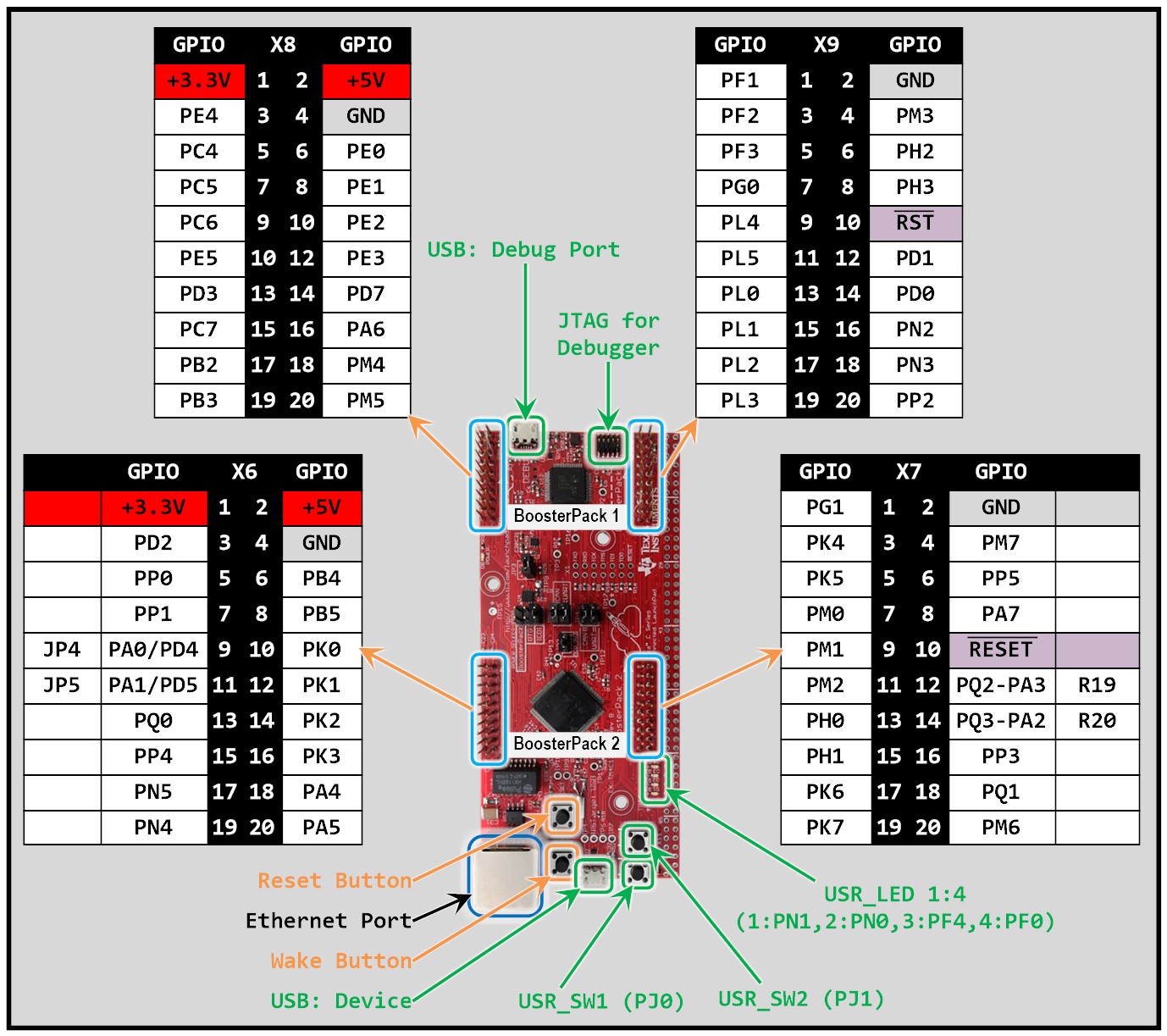
Figure 4: Pinout for the TM4C1294XL LaunchPad
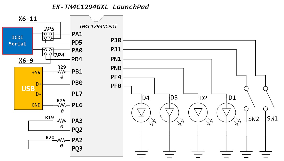
Figure 5: User Switches and RGB LED Signals
Sample Firmware Code in Assembly
Launch Keil μVision5 on your computer, then create a new project. Copy and paste the following source code into your main.s
Please download the definition ZIP file and extract it into the same project folder: TM4C1294NCPDTI.zip
The following source code is to turn on the onboard switches and LEDs on PORTF, PORTN, and PORTJ
;This is the first ARM Assembly language program you see in the lab
;This program template was created by Airs Lin @ 2017 California State University of Los Angeles.
;When you write your program, you could have your info at the top document block
;For Example:  Your Name, Student Number, what the program is for, and what it does etc.

           INCLUDE     TM4C1294NCPDT.s
; Constant Variable Here
STACK_ADDR_123G     EQU     0x20008000
LED1_N              EQU     2_00000010
LED2_N              EQU     2_00000001
LED3_F              EQU     2_00010000
LED4_F              EQU     2_00000001
SW1_J               EQU     2_00000001
SW2_J               EQU     2_00000010

            THUMB

; Vector Table Mapped to Address 0 at Reset
; Linker requires __Vectors to be exported

            AREA    RESET, DATA, READONLY
            EXPORT  __Vectors
__Vectors
            DCD     STACK_ADDR_123G         ; stack pointer value when stack is empty
            DCD     Reset_Handler           ; reset vector

            ALIGN

; The program
; Linker requires Reset_Handler

            AREA    |.text|, CODE, READONLY
            ENTRY                           ; mark first instruction to execute
            EXPORT Reset_Handler
Reset_Handler
; This subroutine grants access to
; floating point coprocessor.
; It is called by the startup code.
            LDR     R0, =0xE000ED88
                    ; Enable CP10,CP11
            LDR     R1,[R0]
            ORR     R1,R1,#0x20
            STR     R1,[R0]
            DSB                             ; wait for store to complete
            ISB                             ;reset pipeline now the FPU is enabled

;=====================
; 1. Turn on Port F clock in SYSCTL_RCGCGPIO_R, tehn check SYSCTL_PRGPIO
; enable clock to GPIOF at clock gating register
            LDR     R0, =SYSCTL_RCGCGPIO_R  ; RCGC reg. addr.
            MOV     R1, #(GPIO_PORTF :OR: GPIO_PORTJ :OR: GPIO_PORTN)
            STR     R1, [R0]

            LDR     R0, =SYSCTL_PRGPIO_R
Wait4GPIO   LDR     R1, [R0]
            TST     R1, #(GPIO_PORTF :OR: GPIO_PORTJ :OR: GPIO_PORTN)
            BEQ     Wait4GPIO

; 2. Unlock PD7 only

; 3. Clear AMSEL to disable analog
            MOV     R1, #0x00
            LDR     R0, =GPIO_PORTF_AHB_AMSEL_R
            STR     R1, [R0]
            LDR     R0, =GPIO_PORTJ_AHB_AMSEL_R
            STR     R1, [R0]
            LDR     R0, =GPIO_PORTN_AHB_AMSEL_R
            STR     R1, [R0]

; 4. Clear PCTL to select GPIO
            MOV     R1, #0x0000
            LDR     R0, =GPIO_PORTF_AHB_PCTL_R
            STR     R1, [R0]
            LDR     R0, =GPIO_PORTJ_AHB_PCTL_R
            STR     R1, [R0]
            LDR     R0, =GPIO_PORTN_AHB_PCTL_R
            STR     R1, [R0]
; 5. Clear AFSEL bits to 0 to select regular I/O
            MOV     R1, #0x00
            LDR     R0, =GPIO_PORTF_AHB_AFSEL_R
            STR     R1, [R0]
            LDR     R0, =GPIO_PORTN_AHB_AFSEL_R
            STR     R1, [R0]
            LDR     R0, =GPIO_PORTJ_AHB_AFSEL_R
            STR     R1, [R0]
; 6. Set DIR to 0 for input, 1 for output
            LDR     R0, =GPIO_PORTF_AHB_DIR_R
            MOV     R1, #(BIT4 :OR: BIT0)   ; PF4 & PF0 to LED
            STR     R1, [R0]
            LDR     R0, =GPIO_PORTN_AHB_DIR_R
            MOV     R1, #(BIT1 :OR: BIT0)   ; PN1 & PN0 to LED
            STR     R1, [R0]
            LDR     R0, =GPIO_PORTJ_AHB_DIR_R
            MOV     R1, #0x00               ; PJ1 & PJ0 to Switch
            STR     R1, [R0]
; 7. Set PUR bits to 1 to enable internal pull-up
            LDR     R0, =GPIO_PORTJ_AHB_PUR_R
            MOV     R1, #(BIT1 :OR: BIT0)
            STR     R1, [R0]
; 8 Set DEN bits to 1 to enable data pins
            LDR     R0, =GPIO_PORTF_AHB_DEN_R
            LDR     R1, [R0]
            ORR     R1, #0x11
            STR     R1, [R0]

            LDR     R0, =GPIO_PORTN_AHB_DEN_R
            LDR     R1, [R0]
            ORR     R1, #0x03
            STR     R1, [R0]

            LDR     R0, =GPIO_PORTJ_AHB_DEN_R
            LDR     R1, [R0]
            ORR     R1, #0x03
            STR     R1, [R0]

;;;;;;;;;; Your Main Code Starts from the next line ;;;;;;;;;;;;


DeadLoop    B       DeadLoop                ; Infinite loop to end program

; The constant variable area
; The value will be stored on ROM segment
            AREA    ConstantVariables, DATA, READONLY
PORT_UNLOCK_CODE    DCD 0x4C4F434B


; The variables area
; The variables will be assigned to RAM area
            AREA    Variables, DATA, READWRITE

            END     ; End of the program
Sample Firmware Code for Keil C
#include <stdio.h>
#include <stdlib.h>
#include <stdint.h>
#include <stdbool.h>

#include "TM4C1294NCPDT.h"

void Setup_GPIO();
void DelayMs(int s);

int main(void)
{
    Setup_GPIO();

    while(1){
        GPIOF_AHB->DATA = 0x01;
        DelayMs(1000);
        GPIOF_AHB->DATA = 0x10;
        DelayMs(1000);
        GPIOF_AHB->DATA = 0x00;
        GPION->DATA = 0x01;
        DelayMs(1000);
        GPION->DATA = 0x02;
        DelayMs(1000);
        GPION->DATA = 0x00;
    }
}
void Setup_GPIO()
{
    // GPIO Initialization and Configuration
    // 1. Enable Clock to the GPIO Modules (SYSCTL->RCGCGPIO |= (_PORTs);)
    SYSCTL->RCGCGPIO |= (_PORTs); |= 0x1020;
    // allow time for clock to stabilize (SYSCTL->PRGPIO)
    while((SYSCTL->PRGPIO & (0x1020) ) != (0x1020) ){};
    // 2. Unlock GPIO only PD7, PF0 on TM4C123G; PD7, PE7 on TM4C1294 (GPIOx->LOCK = 0x4C4F434B; and GPIOx->CR = _PINs;)
    // 3. Set Analog Mode Select bits for each Port (GPIOn[_AHB]->AMSEL 0=digital, 1=analog)
    GPIOF_AHB->AMSEL = 0x00;
    GPION->AMSEL     = 0x00;
    // 4. Set Port Control Register for each Port (GPIOn[_AHB]->PCTL = PMCn, check the PCTL table)
    GPIOF_AHB->PCTL  = 0x00;
    GPION->PCTL      = 0x00;
    // 5. Set Alternate Function Select bits for each Port (GPIOn[_AHB]->AFSEL 0=regular I/O, 1=PCTL peripheral)
    GPIOF_AHB->AFSEL = 0x00;
    GPION->AFSEL     = 0x00;
    // 6. Set the output pins for each port only (Direction of the Pins: GPIOn[_AHB]->DIR 0=input, 1=output)
    GPIOF_AHB->DIR   = 0x11; // PF4,PF0 for Output
    GPION->DIR       = 0x03;
    // 7. Set PUR bits for internal pull-up, PDR for pull-down reg, ODR for open drain
    // 8. Set Digital ENable register on all GPIO pins (GPIOn[_AHB]->DEN 0=disable, 1=enable)
    GPIOF_AHB->DEN   = 0x11; // Enable all digital pins on PortF (PF4, PF0)
    GPION->DEN       = 0x03; // Enable all digital pins on PortN (PN1, PN0)
}
void DelayMs(int s)
{
    volatile int i, j;
    for (i = 0; i < s; i++)
        for (j = 0; j < 3180; j++){};
}
9.2 Setup GPIO
Setup GPIO
When configuring the GPIO registers, the datasheet specifies which bits to set, so the most direct approach is to write a binary or hexadecimal value directly to the register. This compiles and works, but a bare hex number is hard to read while you are debugging. Consider two typical cases.
Case 1 — a register that selects ports. To enable the clock for the ports you use, you write bits into RCGCGPIO:
SYSCTL->RCGCGPIO |= 0x06; /* which ports? */Here, you cannot tell at a glance which ports are being enabled — you have to work out that bit 1 and bit 2 mean Port B and Port C. With macros, the intent is obvious:
SYSCTL->RCGCGPIO |= (_PORTB | _PORTC); /* clearly: Port B and Port C */Case 2 — a register that selects pins. Here, the port is already named by GPIOF->, so the question is which pins:
GPIOF->DIR |= 0x0A; /* Port F is clear -- but which pins? */You still have to decode 0x0A by hand to see that it means pins 1 and 3. The macro version says so directly:
GPIOF->DIR |= (_PIN1 | _PIN3); /* clearly: pins 1 and 3 of Port F */To keep the code readable and easy to maintain, we define all of these names in MyDefines.h and access the registers through them. In short: port-selecting registers (RCGCGPIO, PRGPIO) use _PORTx, while pin-selecting registers (DIR, DEN, AFSEL, …) use _PINx. Every example in this lesson uses these macros (_PORTx, _PINx, _PCTL_PINn, …).
Setup_GPIO() runs only once, right after reset, when almost every GPIO register is already 0 (the only exceptions are the JTAG/SWD and NMI pins). So, for this one-time setup, you can assign the value directly with =, and you do not need "&= ~( )" to clear bits that are already 0.
Two cases are still the exception and use |=:
• SYSCTL->RCGCGPIO — so you keep any port clocks already enabled elsewhere.
• Port C — because PC0–PC3 come out of reset running JTAG/SWD; a plain "=" on a Port C register would clear those bits and can break the debug interface.
When you use "=", write each register once with a single combined mask (for example, GPIOF->DIR = _PIN1 | _PIN2 | _PIN3;) — a second = to the same register would overwrite the first. Reach for &= ~( ) only when you must clear a bit that is not already 0 (Port C, or reconfiguring a pin at run time).
What the registers look like after reset
Before writing any configuration code, it helps to know the state of the GPIO registers right after a reset. Almost everything starts at 0:
| Register | Default after reset | Meaning |
|---|---|---|
| RCGCGPIO (clock) | 0 | Every port clock is disabled |
| AMSEL | 0 | All pins are digital (not analog) |
| PCTL | 0 | All pins are standard GPIO |
| AFSEL | 0 | No alternate function |
| DIR | 0 | All pins are inputs |
| PUR / PDR / ODR | 0 | Pull-up, pull-down, and open-drain are all disabled |
| DEN | 0 | The digital function of every pin is disabled |
Because so much is already 0, you often only need to write the few registers that differ from the default. The table below shows which of the eight steps you can safely skip.
| Step | Can you skip it? |
|---|---|
| Step 3 (AMSEL) | Skip if every pin is digital — nothing is analog. |
| Steps 4 & 5 (PCTL, AFSEL) | Skip if no pin uses an internal digital function (UART, PWM, Timer, …). |
| Step 6 (DIR) | For input pins, no action is needed (inputs are the default); set only the output pins. |
| Step 7 (PUR/PDR/ODR) | Skip if you don't need any internal pull-up/pull-down or an open-drain output. |
| Step 8 (DEN) | Cannot be skipped for any digital pin — the only exception is an analog pin, which is not digital-enabled. |
Steps 1 and 1.1 (enable the clock and wait for it) are always required, and Step 2 (unlock) is needed only when you use one of the commit-locked pins.
There are eight steps to initialize a GPIO port. The examples below configure a typical set of pins on the EK-TM4C123GXL LaunchPad: the three LEDs (Red = PF1, Blue = PF2, Green = PF3) as outputs, and the two push-buttons (SW1 = PF4, SW2 = PF0) as inputs.
Step 1 — Enable the Port Clock
Activate the clock for every GPIO port used in the project by setting its bit in RCGCGPIO. Because _PORTx already equals the correct bit, you can list the port(s) directly.
SYSCTL->RCGCGPIO |= _PORTF; /* enable clock to Port F */Step 1.1 — Allow the clock to stabilize. Wait until the port reports are ready in PRGPIO before touching any of its registers.
while ((SYSCTL->PRGPIO & (_PORTF)) != (_PORTF)) {}; /* wait until Port F is ready */Step 2 — Unlock the Port (only when needed)
A few pins are commit-locked, so they cannot be accidentally reprogrammed. On the TM4C123G the commit-locked pins are PC0–PC3 (JTAG/SWD), PD7 and PF0 (NMI); on the TM4C1294 they are PC0–PC3, PD7 and PE7. To change such a pin, write the magic value to LOCK, then commit the pin in CR.
TM4C123G — unlock PF0 (no wait loop needed on the APB ports):
GPIOF->LOCK = 0x4C4F434B;   /* "LOCK" key -- unlock Port F */
GPIOF->CR  |= _PIN0;        /* commit PF0 (SW2) so it can be changed */
TM4C1294 — unlock PD7 (poll LOCK until it reads 0, then commit; use the GPIOx_AHB name for Ports A–J):
GPIOD_AHB->LOCK = 0x4C4F434B;      /* unlock Port D */
while (GPIOD_AHB->LOCK != 0);      /* wait until the unlock takes effect */
GPIOD_AHB->CR |= _PIN7;            /* commit PD7 */
Locking only affects the AFSEL, PUR, PDR, and DEN registers of those pins — writes to them are ignored until the pin is committed.
Step 3 — Analog Mode Select (AMSEL)
After reset, every pin is digital (AMSEL = 0). Set an AMSEL bit only for a pin that carries an analog signal (for example, an ADC input). If your project has no analog signal, you can skip this step.
For this all-digital example, no write is needed — AMSEL is already 0. You would write it only to make a pin analog, e.g., GPIOE->AMSEL = _PIN3;
Step 4 — Port Control (PCTL)
The PCTL register selects the digital function of each pin using a 4-bit field per pin. 0x0 means regular GPIO (the default after reset). To route a pin to an internal module (UART, PWM, Timer, …), you set the module's PMC value in the pin's field. For this all-digital LED example, no write is needed. When you do configure an alternate function in a one-time setup, assign the combined value directly.
/* not needed here (standard GPIO). Example for an alternate function: */
GPIOA->PCTL = (1 << _PCTL_PIN0) | (1 << _PCTL_PIN1);   // PA0/PA1 = U0RX/U0TX
The PCTL encoding and the per-module PMC values are covered in Lesson 10.
Step 5 — Alternate Function Select (AFSEL)
This works together with Step 4. AFSEL = 0 keeps the pin as regular GPIO (the default); AFSEL = 1 connects the pin to the internal module selected in PCTL. Set or clear AFSEL to match the PCTL configuration.
/* not needed here (standard GPIO). For an alternate function: */
GPIOA->AFSEL = _PIN0 | _PIN1;   // PA0/PA1 use their module (from PCTL)
Step 6 — Direction (DIR)
Setting the DIR bit makes the pin an output; clearing it makes it an input. After resetting, all pins are inputs, so this step only needs to set the output pins.
GPIOF->DIR = (_PIN1 | _PIN2 | _PIN3); /* Red/Blue/Green LEDs as outputs */The buttons SW1 (PF4) and SW2 (PF0) stay as inputs, so they are left out of DIR.
Step 7 — Pull-Up / Pull-Down / Open-Drain (PUR / PDR / ODR)
Configure the pad resistors as needed: an internal pull-up (PUR), a pull-down (PDR), or an open-drain output (ODR). The on-board buttons have no external resistor, so they need an internal pull-up.
GPIOF->PUR = (_PIN0 | _PIN4); /* pull-ups for SW2(PF0), SW1(PF4) */Step 8 — Digital Enable (DEN)
Enable every digital pin used in the project — both inputs and outputs. Analog pins are not digital-enabled; those use AMSEL (Step 3) instead.
GPIOF->DEN = (_PIN0 | _PIN1 | _PIN2 | _PIN3 | _PIN4); /* LEDs + buttons */Set up GPIO — Summary
The whole GPIO initialization at a glance:
| Step | Register | What to do |
|---|---|---|
| 1 | RCGCGPIO | Enable the port clock — |= _PORTx (always) |
| 1.1 | PRGPIO | Wait until the port is ready (always) |
| 2 | LOCK / CR | Unlock only if you use PD7, PF0 (123G) / PD7, PE7 (1294) |
| 3 | AMSEL | Analog select — skip if all pins are digital (reset 0) |
| 4 | PCTL | Function select — skip for plain GPIO (reset 0) |
| 5 | AFSEL | Alternate function — skip for plain GPIO (reset 0) |
| 6 | DIR | Direction — set the output pins only (inputs are the default) |
| 7 | PUR / PDR / ODR | Pull-up/Pull-down/Open-drain — skip if not needed |
| 8 | DEN | Digital enable — every digital pin, in and out (required) |
• Use the MyDefines.h macros: _PORTx for the port-selecting registers (RCGCGPIO, PRGPIO), _PINx for the pin-selecting registers (DIR, DEN, …).
• Because Setup_GPIO() runs once from reset (registers are 0), assign with = and skip anything already 0. Exceptions use |=: RCGCGPIO and Port C (JTAG/SWD).
• With =, write each register once using a single combined mask.
• Register names by board: TM4C123G → GPIOx (APB). TM4C1294 → GPIOx_AHB for Ports A–J, plain GPIOx for Ports K–Q.
• Order: clock → wait → unlock (if needed) → AMSEL → PCTL → AFSEL → DIR → PUR/PDR/ODR → DEN.
9.3 GPIO DATA Register
GPIO DATA Register
The TI TM4C microcontroller features a special register for controlling its pins, known as the DATA register, one for each set of pins, which is referred to as a GPIO (General-Purpose Input/Output) port. You can think of the DATA register as a control panel for eight different pins.
The DATA register is used for two main things:
- To check the current state of the pins. This means you can see which pins are getting power and which are not.
- Set the pins to be either on or off if they are being used as output pins, which function like little lights that can be turned on or off.
Here's how it works when you're using a pin as part of a GPIO port:
- If you are sending information to the pin (like an output), whatever you put in the DATA register tells the pin to turn on or off.
- If you are receiving information into the pin (like an input), reading the DATA register is like asking the pin, "Are you on or off?"
Here are some simple examples to understand how to use it:
- To turn on Pin 2 in Port A (akin to turning a switch on), you would perform an operation like this: take the current settings of Port A and apply a bitwise 'or' with a mask of 1 to enable Pin 2.
GPIOA->DATA = GPIOA->DATA | _BIT2; - To turn off Pin 7 on Port B (similar to switching it off), follow these steps: Take the current Port B settings and apply a bitwise 'and' with the mask 0 to turn off Pin 7.
GPIOB->DATA = GPIOB->DATA & (~_BIT7); - To determine whether Pin 2 on Port D is on or off, follow these steps: Use the bitwise 'and' operator with a mask value of 1 to examine Pin 2 on Port D and verify whether it is receiving power.
if ((GPIOD->DATA & _BIT2) != 0){ } // true: PD2 is logic 1; false: PD2 is logic 0
Remember, the _BIT2 or _BIT7 is just a way of referring to Pin 2 or Pin 7 in the DATA register. It's like saying "Pin number 2" or "Pin number 7".
9.4 Critical Function GPIO Protection
Critical Function GPIO Protection
A few pins on the TM4C devices are protected against accidental reprogramming because they are wired to hardware on which the system depends. There are two such groups:
| Group | TM4C123G | TM4C1294 | Default state after reset |
|---|---|---|---|
| JTAG / SWD | PC3, PC2, PC1, PC0 | PC3, PC2, PC1, PC0 | Already active as JTAG/SWD (AFSEL=1, PCTL=0x1, DEN=1, PUR=1), commit-locked |
| NMI | PD7, PF0 | PD7, PE7 | Plain GPIO (all bits 0), but commit-locked |
Why are these pins locked?
Both groups carry a critical system function. The JTAG/SWD pins are the debug and programming interface — if you reconfigure them by accident, you can lose the ability to flash or debug the board. The NMI (Non-Maskable Interrupt) pins carry an interrupt that, by design, cannot be masked; silently repurposing them could disable a safety-critical input. To prevent an accidental write from breaking either function, TI holds these pins in a commit-locked state out of reset: the corresponding bit in the commit register GPIOCR is 0.
Note the difference between the two groups. The JTAG/SWD pins (PC0–PC3) come out of reset already running the JTAG function. The NMI pins (PD7, PF0 / PE7) come out of reset as ordinary GPIO — but they are still commit-locked, so you must unlock them even to use them as a normal input or output.
What is restricted if you do NOT unlock?
While a pin is commit-locked, any write to the following registers for that pin is silently discarded — the write appears to succeed in your code but the register bit does not change:
- GPIO Alternate Function Select — GPIOn->AFSEL
- GPIO Pull-Up / Pull-Down Select — GPIOn->PUR and GPIOn->PDR
- GPIO Digital Enable — GPIOn->DEN
How to unlock a PIN
Unlocking takes three moves: write the lock key to open the commit register, set the commit bit for the pin(s) you need, then configure the pin as usual. Optionally re-lock afterward. The key 0x4C4F434B (the ASCII letters "LOCK") is the same on both devices. Two board differences to note: on the TM4C1294, use the GPIOx_AHB name for Ports A ~ J and poll LOCK until it reads 0 before committing; on the TM4C123G, the plain GPIOx name is used, and no wait loop is needed.
TM4C123G — unlock PF0 (wired to SW2):
GPIOF->LOCK = 0x4C4F434B;   /* GPIO_LOCK_KEY -- open the commit register */
GPIOF->CR  |= _PIN0;        /* commit PF0 so its config can be changed  */

/* now these writes take effect */
/* PF0 as input  */
GPIOF->PUR  =  _PIN0;       // enable pull-up
GPIOF->DEN  =  _PIN0;       // digital enable

// GPIOF->LOCK = 0;         // re-lock the commit register (optional)
TM4C1294 — unlock PE7 (Port E is in A ~ J, so use GPIOE_AHB, and poll LOCK before committing):
GPIOE_AHB->LOCK = 0x4C4F434B;
while (GPIOE_AHB->LOCK != 0);   // wait until the unlock takes effect
GPIOE_AHB->CR  |= _PIN7;        // commit PE7

GPIOE_AHB->DEN  =  _PIN7;       // ...then configure as needed

//GPIOE_AHB->LOCK = 0;
PD7 exists on both boards, but the code differs by board:
/* TM4C123G */
GPIOD->LOCK = 0x4C4F434B;
GPIOD->CR  |= _PIN7;            // commit PD7

/* TM4C1294 */
GPIOD_AHB->LOCK = 0x4C4F434B;
while (GPIOD_AHB->LOCK != 0);   // wait until the unlock takes effect
GPIOD_AHB->CR  |= _PIN7;        // commit PD7
Reading back GPIOn->LOCK returns the lock status (locked = 1, unlocked = 0). The commit register GPIOCR can only be modified while the LOCK is open.
9.5 GPIO Addressing Masking (Hardware masking address)
GPIO Addressing Masking (Hardware masking address)
If you write an 8-bit value directly to the DATA register, all eight pins will be modified. If you only want to modify specific pins of this port, you must read the values of all pins from the DATA register, use a bitwise operator to change the specific bits, and then write the modified value back to the port. This is called a read-modify-write operation, and it's fraught with issues. For instance, if an interrupt changed the pin state in the middle of this process, your code would write the wrong value to the pin.
In the TI TM4C microcontroller series, there is a clever method for updating only the desired pins without affecting the others: GPIO Address Masking.
On the Tiva TM4C parts, you can use a bit mask to specify which bits to modify. This is done in hardware by mapping each GPIO port to 256 addresses, which covers every possible combination of the port's pins. Bits [9:2] of the address are used as the bit mask.
For example, if we want to change the state of pins 1, 2, and 5 in GPIO Port D, you would create a bit mask where bits 1, 2, and 5 are set to '1' and all other bits are set to '0. In binary, this mask is (0010 0110)2, also called mask 1 value. To use this mask, shift the bit mask value to the left by 2 bits. It will be (00 1001 1000)2 in binary. Then add the GPIO base address to obtain a special address, known as the GPIO masking address. When we write a value to this special address, we instruct the microcontroller to update only pins 1, 2, and 5.
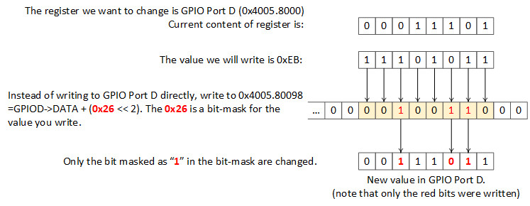
The GPIO addressing mask can be used on input and output pins.
In C code, a pointer can point to hardware-mapped addresses.
 // PD1, PD2 and PD5 are output pins
volatile uint32_t *PD125 = (uint32_t *) GPIOD + (_PIN1 | _PIN2 | _PIN5);

*PD125 = 0xEB;              // Only change pins 1, 2, and 5 on port D
*PD125 = 0;                 // Clear PD1, PD2, PD5 to zero
*PD125 = 0xFF;              // Set PD1, PD2, PD5 to one
*PD125 ^= _BIT1;            // Toggle PD1
Watch the parentheses. Keep the cast on the base address only, so the + stays pointer arithmetic:
(volatile uint32_t *) GPIOD_BASE + n // correct: pointer add, ×4 applied
(volatile uint32_t *)(GPIOD_BASE + n) // wrong: integer add, the ×4 is lost
The base address differs by device and bus: on the TM4C123G, use the APB base (for Port D, GPIOD_BASE). On the TM4C1294, use the AHB base for Ports A ~ J (Port D: GPIOD_AHB_BASE); Ports K ~ Q use their plain GPIOx_BASE.
Read-Modify-Write vs GPIO Address Masking
Before looking at the hardware masking trick, it helps to understand the problem it solves.
What is Read-Modify-Write (RMW)?
To change only a few bits of a register without touching the others, the usual approach is to read the whole register, modify the bits you want, and write the value back. The |= and &= ~ operators you already use are exactly this — a read-modify-write:
GPIOF->DATA |= _PIN1;   /* this one line is really three steps: */
/* 1. Read:   tmp = GPIOF->DATA;   read all 8 pins            */
/* 2. Modify: tmp = tmp | _PIN1;   set bit 1                  */
/* 3. Write: GPIOF->DATA = tmp; write the whole port back */main reads DATA = 0000 0000 → interrupt! ISR does DATA |= _PIN7 → hardware = 1000 0000 main continues: tmp = 0000 0000 | _PIN1 = 0000 0010 main writes DATA = 0000 0010 ← PD7 was wiped out!These bugs are intermittent and hard to find, because they only appear when an interrupt lands in the gap between the read and the write.
How GPIO Address Masking fixes it
The TM4C hardware masking writes the chosen pins in a single, atomic store — there is no read step, so no gap for an interrupt to slip into. The choice of "which pins" is carried by the address (bits [9:2]) instead of by software bit operations:
*PD125 = 0xFF; /* one store instruction; hardware updates only PD1/PD2/PD5 */Comparison
| Read-Modify-Write | GPIO Address Masking | |
|---|---|---|
| Steps | read → modify → write (3) | write (1) |
| Atomic? | No — an interrupt can slip in | Yes for set/clear (single write) |
| Selects pins by | software bit operations | address bits [9:2] |
| Needs a read first | Yes | No |
| Works on | any register | The GPIODATA register only |
| Portability | universal (all MCUs) | TM4C-specific (see note) |
Setting, clearing, and toggling an output
| Operation | Read-Modify-Write | GPIO Address Masking |
|---|---|---|
| Set pins | DATA |= mask; | *p = 0xFF; (atomic) |
| Clear pins | DATA &= ~mask; | *p = 0; (atomic) |
| Toggle pins | DATA ^= mask; | *p = ~*p; |
For toggling, RMW uses ^= with the pin mask, so only those pins flip. With masking, the address already restricts which pins change, so you can simply invert the value read back — *p = ~*p;. (C has no ~= operator; the idiom is x = ~x.)
Checking input pin status
Reading is a single load in both cases, so it is atomic either way — the difference is only whether you filter the pins in software or let the address do it.
| Read-Modify-Write style | GPIO Address Masking |
|---|---|
| val = GPIOF->DATA & mask; | val = *p; |
| Read the whole port, then AND out the pins you want in software | The hardware returns only the masked pins; all other bits read as 0, so no software AND is needed |
/* RMW / plain read: is SW1 (PF4) pressed?  (active-low button) */
if ((GPIOF->DATA & _PIN4) == 0) { /* pressed */ }

/* Masking read: read SW1 (PF4) and SW2 (PF0) together */
volatile uint32_t *SW = (volatile uint32_t *)GPIOF_BASE + (_PIN0 | _PIN4);
uint32_t state = *SW;    /* only the PF0 and PF4 bits are set; all others read 0 */
Use the AHB based on the TM4C1294 (for Port F, GPIOF_AHB_BASE).
Reading a single pin. The cleanest way to test one input is to build a one-bit mask pointer, so the read returns just that pin:
volatile uint32_t *pSw = (volatile uint32_t *)GPIOF + (_PIN4);   /* SW1 = PF4 */

bool sw = *pSw;        /* reads only PF4; all other bits are 0 */

if (sw) {              /* PF4 is high */
    /* Do... */
}• *pSw returns the bit weight, not 0/1 — when PF4 is high it reads 0x10 (16), not 1. Assigning to a bool is fine (any non-zero becomes true), but if you keep it as an integer, test with if (val) or if (val == _PIN4) — never if (val == 1).
• The LaunchPad buttons SW1 (PF4) and SW2 (PF0) are active-low (pressed = 0), so "pressed" is if (!sw).
When to use which
Use GPIO Address Masking when you read or write pin states (the DATA register) and:
- The main code and an interrupt handler may touch different pins of the same port — this is the case that most needs it;
- You want the fastest, single-instruction update;
- You want to pass "these particular pins" around as one pointer.
Use Read-Modify-Write (|= / &= ~) when:
- You configure a register that has no masking address — DIR, DEN, AFSEL, PCTL, PUR, … (this is why Setup_GPIO() uses RMW);
- You are sure no interrupt will change the same port in between (for example, during start-up, or a port only the main loop uses);
- The code must port to other microcontrollers.
Is GPIO Address Masking available on every ARM Cortex-M4?
No. GPIO Address Masking is a feature of the TI Tiva/Stellaris GPIO peripheral (TM4C, LM3S), not of the ARM Cortex-M4 core. ARM defines only the core (pipeline, NVIC, SysTick, bus interfaces); the GPIO peripheral is designed by each chip vendor, so the register layout — and whether masking addresses exist — differs from vendor to vendor.
- STM32 (ST Cortex-M4) lacks an 8-pin masking address; it achieves the same atomic result using the BSRR (Bit Set/Reset Register) instead.
- Other Cortex-M4 families (NXP, Microchip, …) each have their own approach, often dedicated set/clear/toggle registers.
There is also a separate core-level trick called bit-banding that maps each bit to its own word address for atomic single-bit access — but it is optional (not guaranteed on every M4; the TM4C parts do not implement it) and it changes only one bit at a time, whereas TM4C masking can update several pins at once.