
Tiva Lab 01: Blinking LEDs
This lab introduces the fundamentals of embedded programming using the TI Tiva LaunchPad series. Participants gain practical experience with the Keil μVision IDE, GPIO configurations, and bit-wise operations by developing simple firmware to blink onboard LEDs. The lab reinforces the importance of infinite loops in microcontroller applications and lays the groundwork for more complex embedded projects.
Introduction
Embedded systems rely on simple components, such as LEDs, to provide immediate visual feedback and facilitate debugging. This lab uses the TI Tiva LaunchPad boards (EK-TM4C123GXL and EK-TM4C1294XL) to demonstrate core embedded programming concepts. Participants will explore the Keil μVision IDE, practice setting up C projects, and learn how to manipulate GPIO pins using #define statements and bit-wise operations. The lab underscores the importance of continuous loops (e.g., while(1)) in embedded applications, which run independently of an operating system.
Objective
- Project Setup with Keil IDE: Familiarize with the Keil IDE by creating a new C project tailored for the TI Tiva LaunchPad Boards.
- Code Optimization with #define: Utilize #define statements to make the code more understandable and efficient.
- GPIO Configuration Mastery: Learn to set up and control GPIO for output operations, specifically for LED control.
- Bit-wise Operations: Grasp the usage of bit-wise operators to manipulate specific GPIO pins, turning LEDs on or off.
- LED Feedback Control: Reprogram the Tiva board to alter the blinking behavior of its onboard LEDs.
- Understanding Infinite Loops: Comprehend the significance of the "while(1)" loop in embedded systems and its necessity for continuous operation.
Required Reading Materials
- Lesson 07: Create an ARM C Application with Keil μVision MDK-ARM
- Lesson 09: GPIO Ports and Configurations
- Set, Clear, Toggle, and Check Bit Value in C
- Polling Method in Embedded Programming
Components Required
| Component/Device | Description | Quantity |
|---|---|---|
 |
TM4C1294 onboard Green LEDs (LED1 ~ LED4) | × 4 |
  |
TM4C123G onboard RGB LED | × 1 |
Background
The Tiva launchPad has rows of connectors along both sides that connect to several electronic devices and plug-in 'shields' that extend its capability. The EK-TM4C123GXL LaunchPad has a single RGB LED on the board, and the EK-TM4C1294XL LaunchPad has four LEDs. Those can be used on your embedded applications. The onboard LEDs may blink when you first connect the board to a USB plug. That is because the boards are generally shipped with the Blink sketch pre-installed.
In this lab, we will reprogram the Tiva board with our Blink code and then adjust the blink rate.
Please follow Lesson 07: Create an ARM C Application with Keil μVision MDK-ARM to learn how to set up the Keil μVision IDE, create a new project, download and debug the code.
Circuit Diagram
The onboard switches and LEDs for Tiva LaunchPads are as shown below:
EK-TM4C123GXL LaunchPad - Circuit
The EK-TM4C123GXL LaunchPad comes with an RGB LED and two user buttons. Table 1 shows how these features are connected to the microcontroller's pins.
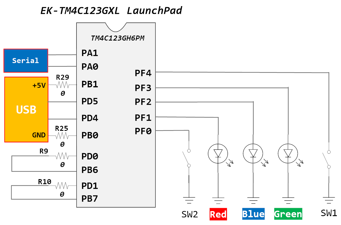
Table 1: User Switches and RGB LED Signals
| GPIO Pin | Pin Function | User Device |
| PF4 | GPIO | SW1 |
| PF0 | GPIO | SW2 |
| PF1 | GPIO | RGB LED (Red) |
| PF2 | GPIO | RGB LED (Blue) |
| PF3 | GPIO | RGB LED (Green) |
Table2: Pin Configurations for TM4C123G
| Device | Port.Pin | Signal Type | PCTL | Direction | Drive Mode |
|---|---|---|---|---|---|
In your code, you must configure GPIO Port F, pins 1 and 3, as outputs.
EK-TM4C1294XL LaunchPad - Circuit
The EK-TM4C1294XL LaunchPad comes with four green LEDs and two user buttons. Table 2 shows how these features are connected to the microcontroller's pins. Note that the four LEDs are split across two ports (Port N and Port F).
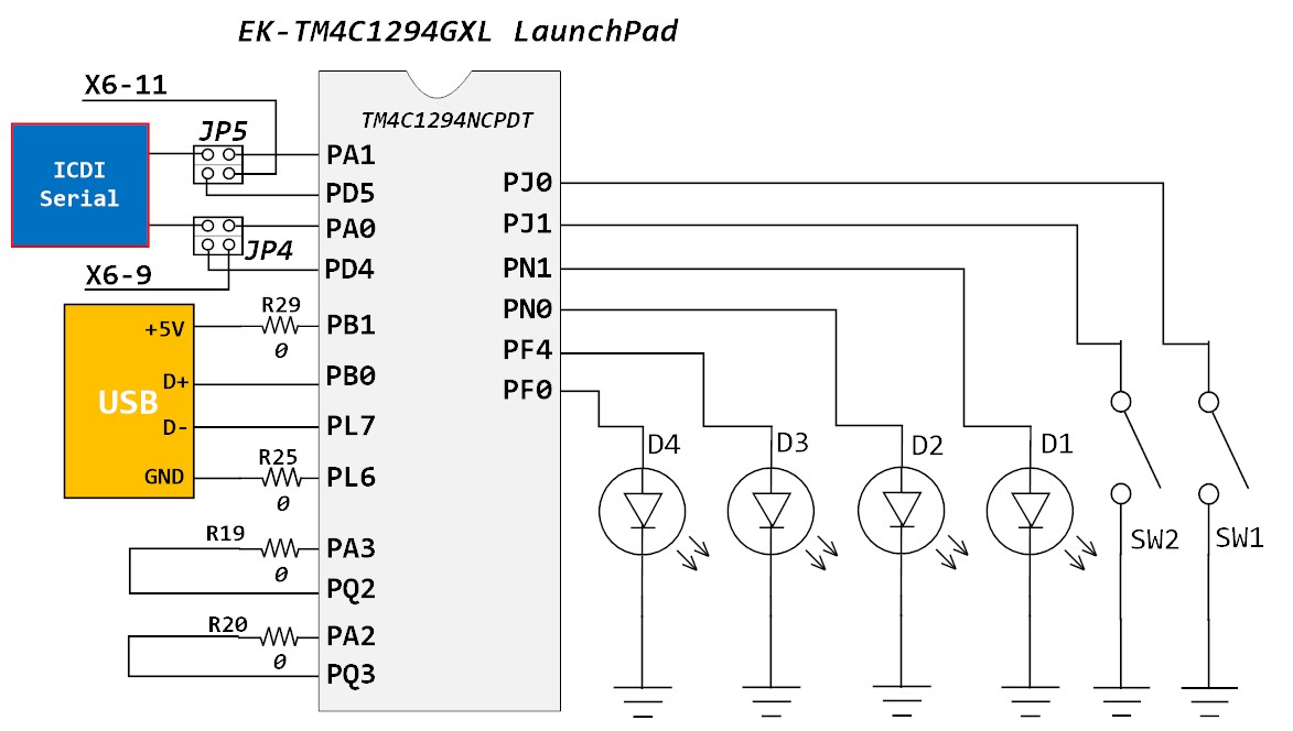
Table 3: User Switches and Green LED Signals
| GPIO Pin | Pin Function | User Device |
| PJ0 | GPIO | SW1 |
| PJ1 | GPIO | SW2 |
| PN1 | GPIO | LED1 (D1) |
| PN0 | GPIO | LED2 (D2) |
| PF4 | GPIO | LED3 (D3) |
| PF0 | GPIO | LED4 (D4) |
Table 4: Pin Configurations for TM4C1294
| Device | Port.Pin | Signal Type | PCTL | Direction | Drive Mode |
|---|---|---|---|---|---|
In your code, you must configure PN1, PN0 (Port N), and PF4, PF0 (Port F) as outputs. Because the LEDs span two ports, remember to enable the clock for both ports.
Procedure
In this lab, you will create a C project for the Tiva LaunchPad, add the shared macro header, configure the GPIO port, and blink the on-board LEDs.
Before starting, study Lesson 07: Create an ARM C Application with Keil μVision MDK-ARM, which covers creating a project, selecting a device, and downloading/debugging code.
Part 1 — Create the Project
- Under your EE3450 folder, create a new folder named Lab01_BlinkingLEDs and open it. This folder will hold this lab's project files.
- Launch Keil μVision and create a new project. When prompted, select the device that matches your board — TM4C123GH6PM for the EK-TM4C123GXL, or TM4C1294NCPDT for the EK-TM4C1294XL. Save the project as Lab01_BlinkingLEDs. (See Lesson 07 for the full walkthrough.)
Part 2 — Add the Shared MyDefines.h Header
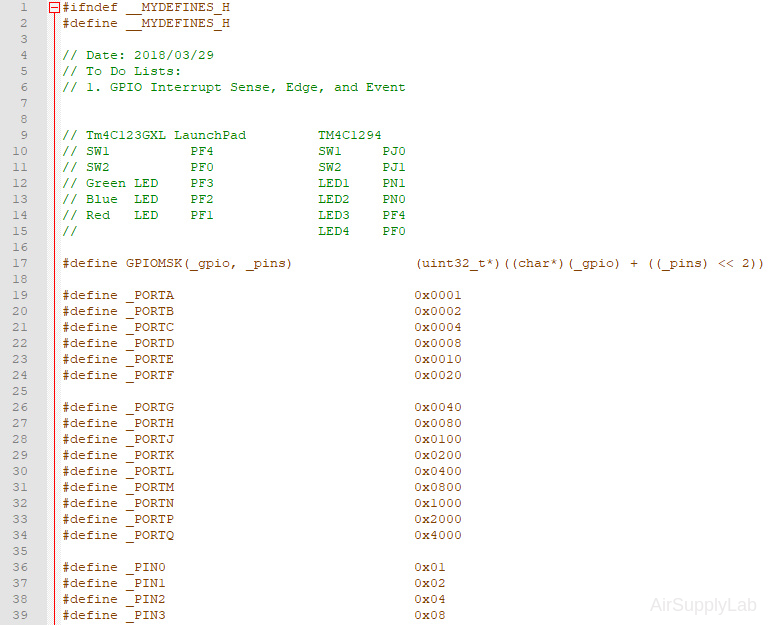
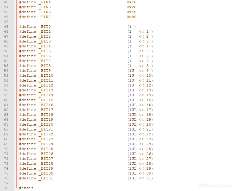
- Type in the MyDefines.h file and save it in your Common folder. Enter it yourself rather than copying it — typing the macros is how you learn them.
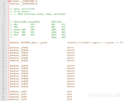
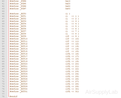
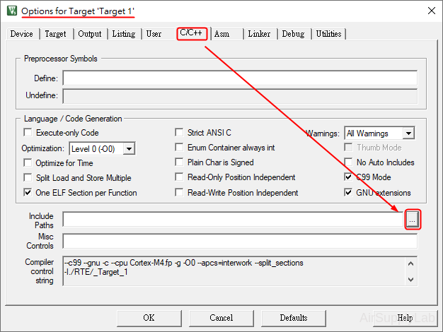
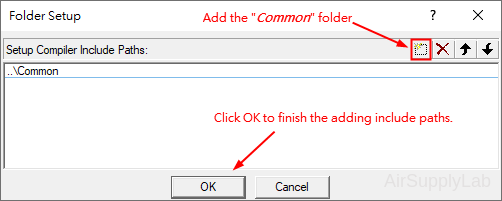
- Tell the compiler where to find the MyDefines.h header file: open Options for Target → C/C++ tab, and add the Common folder to the Include Paths field. Click OK.
Part 3 — Add the Template Firmware
- Copy the provided incomplete main.c template into your project (use the file for your board). Unlike MyDefines.h — which you type in yourself to learn the macros — you simply copy this file: it already contains the boilerplate so you can focus on the two parts you will complete yourself, the Setup_GPIO() function (Part 4) and the while(1) loop (Part 5).
Lab Template Firmware Source Code
This section provides the template firmware source code for the TM4C123G and TM4C1294 platforms used in these laboratory exercises. Explanatory notes are included to help readers understand the purpose and operation of each major part of the program.
The provided code is intended as a reference starting point and may be copied into the project as needed. Since the template is not a final, complete program, it should be reviewed and modified to meet the requirements of each experiment. Unnecessary statements may be commented out, and appropriate comments should be added to clearly document the program structure and implementation details.
EK-TM4C123GXL LaunchPad - main.c
#include <stdio.h>
#include <stdlib.h>
#include <stdint.h>
#include <stdbool.h>

#include "TM4C123GH6PM.h"
#include "MyDefines.h"

void DelayMs(int ms);   // Software Delay Function
void Setup_GPIO(void);

int main(void)
{
    // Place your initialization/startup code here (e.g. Setup_GPIO() )
    Setup_GPIO();

    while (1) {
        // Place your application code here

    }
}
//------------------------------------------------------------------------------
/*
Device      Port.Pins       DIR     DriveMode
LEDR
LEDG
SW1
SW2

Port ____
*/

void Setup_GPIO(void)
{
    // Configure GPIOs
    // 1. Enable Clock to the GPIO Modules (SYSCTL->RCGCGPIO |= (_PORTs);)
    SYSCTL->RCGCGPIO |= (__);
    // allow time for clock to stabilize (SYSCTL->PRGPIO & (_PORTs))
    while ((SYSCTL->PRGPIO & (__)) != (__)) {};
    // 2. Unlock GPIO only PD7, PF0 on TM4C123G; PD7, PE7 on TM4C1294 (GPIOx->LOCK = 0x4C4F434B; and GPIOx->CR = _PINs;)
    // Unlock PF0
    GPIOF->LOCK = 0x4C4F434B;   // Unlock for GPIOF
    GPIOF->CR |= _PIN0;         // Commit for PIN0
    // 3. Set Analog Mode Select bits for each Port (GPIOx->AMSEL = _PINs;)
    // 4. Set Port Control Register for each Port (GPIOx->PCTL = PMCn << _PTCL_PINn, check the PCTL table)
    // 5. Set Alternate Function Select bits for each Port (GPIOx->AFSEL = _PINs;)
    // 6. Set the output pins for each port only (Direction of the Pins: GPIOx->DIR = _PINs;)

    // 7. Set PUR bits (internal Pull-Up Resistor), PDR (Pull-Down Resistor), ODR (Open Drain) for each Port

    // 8. Set Digital ENable register on all digital port.pins (GPIOx->DEN = _PINs;)

}
//------------------------------------------------------------------------------
// Delay ms milliseconds (4167:50MHz TM4C123G CPU, 1605:16MHz TM4C123G CPU Clock)
void DelayMs(int ms)
{
    volatile int i, j;
    for (i = 0; i < ms; i++)
        for (j = 0; j < 4167; j++) {} // Do nothing for 1ms
}
EK-TM4C1294XL LaunchPad - main.c
#include <stdio.h>
#include <stdlib.h>
#include <stdint.h>
#include <stdbool.h>

#include "TM4C1294NCPDT.h"
#include "MyDefines.h"

void DelayMs(int ms);   // Software Delay Function
void Setup_GPIO(void);

int main(void)
{
    // Place your initialization/startup code here (e.g. Setup_GPIO() )
    Setup_GPIO();
    while (1) {
        // Place your application code here

    }
}
//------------------------------------------------------------------------------
/*
Device      Port.Pins       DIR     DriveMode
LED1
LED2
SW1
SW2

Port ____
*/
void Setup_GPIO(void)
{
    // Configure GPIOs
    // 1. Enable Clock to the GPIO Modules (SYSCTL->RCGCGPIO |= (_PORTs);)
    SYSCTL->RCGCGPIO |= (__);
    // allow time for clock to stabilize (SYSCTL->PRGPIO & (_PORTs))
    while ((SYSCTL->PRGPIO & (__)) != (__)) {};
    // 2. Unlock GPIO only PD7, PF0 on TM4C123G; PD7, PE7 on TM4C1294 (GPIOx->LOCK = 0x4C4F434B; and GPIOx->CR = _PINs;)
    // Unlock PD7
    // GPIOD_AHB->LOCK = 0x4C4F434B;
    // while (GPIOD_AHB->LOCK != 0);
    // GPIOD_AHB->CR |= _PIN7;
    // 3. Set Analog Mode Select bits for each Port (GPIOx->AMSEL = _PINs;)
    // 4. Set Port Control Register for each Port (GPIOx->PCTL = PMCn << _PTCL_PINn, check the PCTL table)
    // 5. Set Alternate Function Select bits for each Port (GPIOx->AFSEL = _PINs;)
    // 6. Set the output pins for each port only (Direction of the Pins: GPIOx->DIR = _PINs;)

    // 7. Set PUR bits (internal Pull-Up Resistor), PDR (Pull-Down Resistor), ODR (Open Drain) for each Port

    // 8. Set Digital ENable register on all digital port.pins (GPIOx->DEN = _PINs;)

}
//------------------------------------------------------------------------------
// Delay ms milliseconds (1605: 16MHz TM4C1294 CPU Clock)
void DelayMs(int ms)
{
    volatile int i, j;
    for (i = 0; i < ms; i++)
        for (j = 0; j < 1605; j++) {}   // // Do nothing for 1ms
}
- Copy-paste the following code to your main.c file.
- Modify the Setup_GPIO() function based on the Pin Configuration Table (table 2 or 4) to configure the onboard switches and LEDs.
GPIO Initialization and Configuration
GPIO Initialization Configuration
Next, we need to configure all the GPIO ports and pins that are used in the design.
According to the pin connections, complete the following GPIO configurations for each port. Fills the pin field by the value below:
- 0: Clean the bit
- 1: Set the bit
- x: Do not change the bit
- d: Do not care
For both TM4C123GXL and TM4C1294XL LaunchPads, the Port C [3:0] are used for JTAG/SWD. Therefore, when configuring Port C, use bitwise operators to ensure your new configuration settings do not affect the JTAG/SWD function (PC3 ~ PC0).
Most of the GPIO pins are configured as GPIOs and tri-stated by default (GPIOPCTL = 0, CPIOAFSEL = 0, GPIODIR = 0, GPIOPUR = 0, GPIOPDR = 0, GPIOODR = 0)
- Enable Clock to the GPIO Modules (RCGCGPIO register)
TM4C123G: SYSCTL->RCGCGPIO |= (_PORTs); |= binary = hex
8 4 2 1 8 4 2 1 7 6 5 4 3 2 1 0 bit Port F Port E Port D Port C Port B Port A port 0 0 -
TM4C1294: SYSCTL->RCGCGPIO |= (_PORTs); |= binary = hex
After enabling the clock signal, check the PRGPIO register until the corresponding bit is set to 1.8 4 2 1 8 4 2 1 8 4 2 1 8 4 2 1 15 14 13 12 11 10 9 8 7 6 5 4 3 2 1 0 bit Port Q Port P Port N Port M Port L Port K Port J Port H Port G Port F Port E Port D Port C Port B Port A port 0 - - -
In Assembly:
            LDR     R0, =SYSCTL_PRGPIO_R
Wait4GPIO   LDR     R1, [R0]
            TST     R1, #(__)
            BEQ     Wait4GPIO
In c:
while ( (SYSCTL->PRGPIO & ____ ) != ____ ) {}; - Unlock Port
TM4C123G: PD7 and PF0 are locked after reset.
TM4C1294: PD7 and PE7 are locked after reset
If those pins are used in the design, they must be unlocked first. To unlock the port, 0x4C4F434B must be written into the GPIOLOCK register and uncommitted by setting the GPIOCR register.
8 4 2 1 8 4 2 1 7 6 5 4 3 2 1 0 bit Port Pin 7 Pin 6 Pin 5 Pin 4 - Pin 3 Pin 2 Pin 1 Pin 0 pin Value in Hex Register Value to Register - - = ➤ GPIO ->LOCK = 0x4C4F434B - - = ➤ GPIO ->CR - - = ➤ GPIO ->LOCK = 0x4C4F434B - - = ➤ GPIO ->CR
Convert the above configuration into registers
- GPIO Analog Mode Select
If any pin is used as an Analog signal (check the Signal Type field on table 1), the appropriate bit in AMSEL must be set.
- 0: Digital signal
- 1: Analog signal
8 4 2 1 8 4 2 1 7 6 5 4 3 2 1 0 bit Port Pin 7 Pin 6 Pin 5 Pin 4 - Pin 3 Pin 2 Pin 1 Pin 0 pin Value in Hex Register Value to Register - - = ➤ GPIO ->AMSEL - - = ➤ GPIO ->AMSEL - - = ➤ GPIO ->AMSEL - - = ➤ GPIO ->AMSEL - - = ➤ GPIO ->AMSEL - - = ➤ GPIO ->AMSEL - - = ➤ GPIO ->AMSEL - GPIO Port Control (PCTL)
The PCTL register selects the specific peripheral signal for each GPIO pin in alternate function mode.
- 0: GPIO
- 1~0xF: Check the GPIO Pins and Alternate Function table
8421 8421 8421 8421 8421 8421 8421 8421 31~28 27~24 23~20 19~16 15~12 11~8 7~4 3~0 bit Port Pin 7 Pin 6 Pin 5 Pin 4 - Pin 3 Pin 2 Pin 1 Pin 0 pin Value in Hex Register Value to Register - - = ➤ GPIO ->PCTL - - = ➤ GPIO ->PCTL - - = ➤ GPIO ->PCTL - - = ➤ GPIO ->PCTL - - = ➤ GPIO ->PCTL - - = ➤ GPIO ->PCTL - - = ➤ GPIO ->PCTL - GPIO Alternate Function Select (AFSEL)
Setting a bit in the AFSEL register configures the corresponding GPIO pin to be controlled by PCTL peripheral function.
- 0: General I/O
- 1: Pin connected to the digital function defined in the PCTL register
8 4 2 1 8 4 2 1 7 6 5 4 3 2 1 0 bit Port Pin 7 Pin 6 Pin 5 Pin 4 - Pin 3 Pin 2 Pin 1 Pin 0 pin Value in Hex Register Value to Register - - = ➤ GPIO ->AFSEL - - = ➤ GPIO ->AFSEL - - = ➤ GPIO ->AFSEL - - = ➤ GPIO ->AFSEL - - = ➤ GPIO ->AFSEL - - = ➤ GPIO ->AFSEL - - = ➤ GPIO ->AFSEL - GPIO Pin Direction (DIR)
Set pin direction
- 0: Input pin
- 1: Output pin
8 4 2 1 8 4 2 1 7 6 5 4 3 2 1 0 bit Port Pin 7 Pin 6 Pin 5 Pin 4 - Pin 3 Pin 2 Pin 1 Pin 0 pin Value in Hex Register Value to Register - - = ➤ GPIO ->DIR - - = ➤ GPIO ->DIR - - = ➤ GPIO ->DIR - - = ➤ GPIO ->DIR - - = ➤ GPIO ->DIR - - = ➤ GPIO ->DIR - - = ➤ GPIO ->DIR - Internal Pull-Up Resistor (PUR), Pull-Down Resistor (PDR), and Open-Drain (ODR)
PUR: The pull-up control register
PDR: The pull-down control register
ODR: The open-drain control register
- 0: Disable
- 1: Enable
8 4 2 1 8 4 2 1 7 6 5 4 3 2 1 0 bit Port Pin 7 Pin 6 Pin 5 Pin 4 - Pin 3 Pin 2 Pin 1 Pin 0 pin Value in Hex Register Value to Register - - = ➤ GPIO -> - - = ➤ GPIO -> - - = ➤ GPIO -> - - = ➤ GPIO -> - - = ➤ GPIO -> - - = ➤ GPIO -> - - = ➤ GPIO -> - GPIO Digital Enable
Enables all pins used in the design, including GPIO and alternate-function pins.
- 0: Pin undriven
- 1: Enable pin
8 4 2 1 8 4 2 1 7 6 5 4 3 2 1 0 bit Port Pin 7 Pin 6 Pin 5 Pin 4 - Pin 3 Pin 2 Pin 1 Pin 0 pin Value in Hex Register Value to Register - - = ➤ GPIO ->DEN - - = ➤ GPIO ->DEN - - = ➤ GPIO ->DEN - - = ➤ GPIO ->DEN - - = ➤ GPIO ->DEN - - = ➤ GPIO ->DEN - - = ➤ GPIO ->DEN
- Inside the while(1) loop, the commands first turn the LED pin on (high), then delay for 1000 milliseconds (1 second), then turn the LED pin off, and pause for another second.
EK-TM4C123GXL LaunchPad - while loop
Blinking the Red LED
EK-TM4C1294XL LaunchPad - while loop
Blinking the LED1
Every C program must have a main() function, which serves as the program's entry point. In the main() function, the while(1) loop is the most commonly used in embedded microcontroller applications. The line while(1) creates an infinite loop that never stops executing. It executes over and over and over again unless the program is intentionally stopped or there is some condition under this loop that gets met that takes it out of this infinite loop.
Why do embedded programs contain an infinite loop? While personal computers have an operating system, embedded microcontrollers generally do not. Once a program has executed on a personal computer, it returns control to the computer's operating system when it finishes. An embedded microcontroller, however, does not have an operating system and cannot be allowed to fall out of the program at any time. Hence, every embedded microcontroller application has an infinite loop built into it somewhere, such as the line while(1). This prevents the program from running out of things to do and doing random things that may be undesirable.
Lab Experiments
Exp #1.1: Blinking Red and Green LEDs
Exp #1.1: Blinking Red and Green LEDs
This is your first hands-on experiment. You will make two on-board LEDs blink alternately — when one is on, the other is off, and after a short delay, they swap. On the TM4C123G these are the Red and Green LEDs; on the TM4C1294 there is no color, so we simply alternate two of its LEDs.
Your first three tools for controlling outputs: set a bit to turn an LED on, clear a bit to turn it off, and repeat the pattern forever with a while(1) loop and a delay. Every later experiment builds on exactly these ideas.
Objective
- Turn a single LED on by setting its bit, and off by clearing its bit.
- Repeat an action endlessly with a while(1) loop and a delay.
- Control two LEDs independently, so they alternate.
Background — Set and Clear
An output pin is turned on by setting its bit to 1 and turned off by clearing it to 0. In C, we do this without disturbing the other pins of the port:
| Action | Operator | Meaning |
|---|---|---|
| Turn the LED on (set) | PORT->DATA |= LED; | OR the bit in |
| Turn the LED off (clear) | PORT->DATA &= ~LED; | AND the bit out |
Pin Mapping
| TM4C123G | TM4C1294 | |
|---|---|---|
| LED1 | Red, PF1 (_PIN1) | D1, PN1 (_PIN1) |
| LED2 | Green, PF3 (_PIN3) | D2, PN0 (_PIN0) |
Both LEDs are on one port — Port F on the TM4C123G, Port N on the TM4C1294.
Algorithm — Flowchart
LED1 = Red / D1, LED2 = Green / D2. The loop never ends, so the two LEDs keep swapping forever.
Algorithm — Pseudocode
Setup_GPIO()
WHILE (forever)
    set LED1  ,  clear LED2        // LED1 on, LED2 off
    Delay(500 ms)
    clear LED1 ,  set LED2         // LED1 off, LED2 on
    Delay(500 ms)
END WHILE
Your Task
- Call Setup_GPIO() (defined in the Procedure section) so that both LED pins are outputs. Build the masks from the _PINx macros and enable the port clock with _PORTx — do not write raw hex numbers.
- Inside, while(1), set one LED and clear the other, wait, then swap.
- Use the Delay_ms() helper provided in your project template for the wait.
Hint: to turn a pin on, use PORT->DATA |= LED; and to turn it off, use PORT->DATA &= ~LED; — these leave all the other pins untouched.
Expected Result
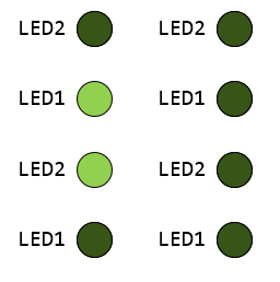
The two LEDs blink back and forth like a railroad-crossing signal: LED1 on / LED2 off, then LED1 off / LED2 on, half a second each, forever.
1. Make both LEDs blink together (both on, both off) instead of alternating.
2. Make the on-time and off-time unequal — for example, on for 800 ms, off for 200 ms.
3. Add a third LED to the pattern (the Blue LED on the TM4C123G, or another LED on the TM4C1294).

Blinking LEDs on TM4C123G Board
Blinking LEDs on TM4C1294 Board
Exp #1.2: LED Binary Up-Counter
Exp #1.2: LED Binary Up-Counter
In Exp #1.1, you turned a single LED on and off. In this experiment, you will drive several LEDs simultaneously so they display an incrementing binary number. Each LED corresponds to a bit, and the pattern on the board is exactly the binary representation of a variable. The counter increases by one every second and wraps back to zero after it overflows.
Until now, you controlled one pin at a time. Here, write a value onto a group of pins without disturbing the other pins on the port, using the clear-then-set (read-modify-write) technique from your reading "Set, Clear, Toggle, and Check Bit Value in C". You will also see why the physical LED-to-pin mapping matters.
Objective
- Represent a numeric value as a pattern of LEDs (binary counting).
- Write several output bits at once without changing the other bits of the port (masked write).
- Drive LEDs spread across multiple GPIO ports.
Pin Mapping
EK-TM4C123GXL — the RGB LED gives us three bits, so the counter runs from 0 to 7.
| Counter Bit | GPIO Pin | LED |
|---|---|---|
| bit 0 (LSB) | PF1 | RGB Red |
| bit 1 | PF2 | RGB Blue |
| bit 2 (MSB) | PF3 | RGB Green |
EK-TM4C1294XL — the four green LEDs give us four bits, so the counter runs from 0 to 15.
| Counter Bit | GPIO Pin | LED |
|---|---|---|
| bit 0 (LSB) | PN1 | D1 |
| bit 1 | PN0 | D2 |
| bit 2 | PF4 | D3 |
| bit 3 (MSB) | PF0 | D4 |
D1 and D2 are on Port N (PN1, PN0) while D3 and D4 are on Port F (PF4, PF0), and the bits are not adjacent. You therefore cannot write a single 4-bit value to a single register; you must place each bit on its own pin. Note also that on the TM4C1294, PF0 is not a locked pin, so no unlock step is required — unlike SW2/PF0 on the TM4C123G.
Algorithm — Flowchart
MAX = 7 on the TM4C123G (3 LEDs), MAX = 15 on the TM4C1294 (4 LEDs). Notice the loop never ends — this is the while(1) infinite loop from Exp #1.1.
Algorithm — Pseudocode
Main program:
count ← 0
Setup_GPIO()                        // set all LED pins as outputs
WHILE (forever)
    DisplayCount(count)             // show the value on the LEDs
    Delay(1000 ms)
    count ← count + 1
    IF count > MAX THEN
        count ← 0                   // MAX = 7 (TM4C123G) or 15 (TM4C1294)
    END IF
END WHILE
To display the value, examine each bit of the counter in turn. If a bit is 1, turn its LED on; if the bit is 0, turn its LED off. The very same method works on both boards.
DisplayCount(value):
    IF bit 0 of value is 1  THEN  turn its LED ON   ELSE  turn its LED OFF
    IF bit 1 of value is 1  THEN  turn its LED ON   ELSE  turn its LED OFF
    IF bit 2 of value is 1  THEN  turn its LED ON   ELSE  turn its LED OFF
    // the TM4C1294 has a fourth LED, so add one more line:
    IF bit 3 of value is 1  THEN  turn its LED ON   ELSE  turn its LED OFF
Use the Pin Mapping table to find which pin each bit controls. Follow the house rule: use the macros in MyDefines.h, not raw hex numbers. To test a single counter bit, AND the value with a bit macro — _BIT0 tests bit 0, _BIT1 tests bit 1, and so on.
Your Task
- Complete Setup_GPIO() using the fill-in tables in the Procedure section, so that every LED pin listed in the Pin Mapping is configured as an output. On the TM4C1294, remember to enable the clock for both Port N and Port F (_PORTF | _PORTN).
- Translate the flowchart/pseudocode into C inside main().
- Write your own DisplayCount() that tests each counter bit and sets or clears the mapped LED pin.
- Reuse the same delay routine you wrote in Exp #1.1.
Hint: The counter bit number and the LED pin number are usually different. For example, counter bit 0 controls PF1 on the TM4C123G, but PN1 on the TM4C1294. Always test the counter bit first, then set or clear the exact pin shown in the Pin Mapping table.
Expected Result
The LEDs should count upward in binary, one step per second. On the TM4C1294, you will see 0000, 0001, 0010, 0011 … up to 1111, then restart from 0000. The least-significant LED toggles every second, the next LED every two seconds, the next every four seconds, and so on — a direct, visible picture of how binary place value works.
1. Turn the program into a down-counter (7→0 on the TM4C123G, 15→0 on the TM4C1294).
2. Increase the speed to four counts per second, and confirm that each LED toggles half as often as the one to its right.
3. (TM4C123G) Since the three LEDs are Red, Blue and Green, write down the color you actually see for each value from 0 to 7.
Exp #1.3: RGB Color Mixer (TM4C123G) / Larson Scanner (TM4C1294)
Exp #1.3: RGB Color Mixer (TM4C123G) / Larson Scanner (TM4C1294)
This experiment is split by board because the two LaunchPads have different LEDs. The TM4C123G has a single three-color RGB LED, so we will mix colors. The TM4C1294 has four LEDs in a row, so we will make a single dot of light sweep back and forth — the "Larson scanner" effect made famous by Knight Rider and Cylon robots.
Part A introduces the bitwise OR to combine single-color LEDs into new colors, and a const array to hold a sequence you step through. Part B introduces a moving position together with a direction variable that reverses at each end — your first taste of a program that "remembers" which way it is going.
Objective
- Combine single-color LED bits with bitwise OR to create new colors.
- Step through a sequence of patterns stored in an array.
- Track a moving position and a direction, reversing at the boundaries.
Part A — TM4C123G: RGB Color Mixer
Part A — TM4C123G: RGB Color Mixer
Pin Mapping
| color | GPIO Pin | MyDefines.h Macro |
|---|---|---|
| Red | PF1 | _PIN1 |
| Blue | PF2 | _PIN2 |
| Green | PF3 | _PIN3 |
How Colors Are Made
The RGB LED has only three primary colors, but turning on more than one at the same time mixes them. Combine the primary masks with the bitwise OR operator (|):
| Mixed color | Combination |
|---|---|
| Yellow | Red | Green |
| Cyan | Green | Blue |
| Magenta | Red | Blue |
| White | Red | Green | Blue |
Algorithm — Pseudocode
Store the color sequence in an array, then step through it in an endless loop:
colors[] = { RED, YELLOW, GREEN, CYAN, BLUE, MAGENTA, WHITE, OFF }
i ← 0
Setup_GPIO()
WHILE (forever)
    ShowColor(colors[i])          // display the next color
    Delay(500 ms)
    i ← i + 1
    IF i ≥ NUM_COLORS THEN i ← 0
END WHILE

ShowColor(c):
    turn all three LEDs OFF
    turn ON the LEDs that are set in c     // the OR pattern lights up
Notice the loop has the same shape as the Exp #1.2 flowchart — only the action inside changes (show a color instead of a number).
Part B — TM4C1294: Larson Scanner
Part B — TM4C1294: Larson Scanner
Pin Mapping
| Position | LED | GPIO Pin | MyDefines.h Macro |
|---|---|---|---|
| 0 | D1 | PN1 | _PIN1 (Port N) |
| 1 | D2 | PN0 | _PIN0 (Port N) |
| 2 | D3 | PF4 | _PIN4 (Port F) |
| 3 | D4 | PF0 | _PIN0 (Port F) |
The Idea
Keep two variables: pos (which LED is lit, 0–3) and dir (which way it is moving, +1 or −1). Each step, light only the LED at pos, then move: pos = pos + dir. When you reach either end, flip the direction with dir = -dir so the dot bounces back.
Algorithm — Flowchart
"Reached an end?" means pos == 0 or pos == LAST_LED (3). Because the dot only meets an end while heading toward it, simply flipping dir makes it bounce.
Algorithm — Pseudocode
pos ← 0                 // which LED is lit (0..3)
dir ← +1                // moving up (+1) or down (-1)
Setup_GPIO()
WHILE (forever)
    LightOne(pos)          // light only LED[pos], all others off
    Delay(100 ms)
    pos ← pos + dir
    IF pos = 0 OR pos = LAST_LED THEN
        dir ← -dir      // bounce: reverse direction
    END IF
END WHILE

LightOne(index):
    turn ALL four LEDs OFF
    turn ON only the LED for this index    // use the Pin Mapping table
Your Task
- Choose the part that matches your board and complete Setup_GPIO() so every LED pin is an output (the TM4C1294 needs both _PORTN | _PORTF).
- Build your color or LED masks from the _PINx macros — do not write raw hex numbers.
- Translate the pseudocode (and, for Part B, the flowchart) into C.
- Reuse the delay routine from Exp #1.1.
Hint (Part B): because the four LEDs live on two different ports (N and F), LightOne() cannot just shift one bit. Clear all four LEDs first, then switch on the single one that matches the index.
Expected Result
TM4C123G: the RGB LED cycles through red, yellow, green, cyan, blue, magenta, white, then off, and repeats — changing color twice per second.
TM4C1294: a single lit LED slides D1→D2→D3→D4, then back D4→D3→D2→D1, bouncing smoothly at both ends.
1. (TM4C1294) Change the scanner so the dot wraps around (D1→D2→D3→D4→D1…) instead of bouncing.
2. (TM4C1294) Make a two-LED "comet": light the current LED and the one just behind it.
3. (TM4C123G) Make the colors ping-pong (forward then backward) by borrowing the dir idea from Part B.
Exp #1.4: SOS Morse Code Beacon
Exp #1.4: SOS Morse Code Beacon
In this experiment, a single LED flashes the international distress signal SOS in Morse code — three short flashes, three long flashes, three short flashes — over and over. The new idea is timing: the pattern is not just on/off, but how long the LED stays on and how long the gaps last.
You will encode a message as a timed sequence of pulses, using two different on-durations (a short dot and a long dash) and structured gaps between them. You will also break the behavior into small, reusable functions — Dot(), Dash(), and the gaps — instead of writing a single long block.
Objective
- Produce two different on-times from the same LED (short dot vs long dash).
- Insert correctly-sized gaps between elements, letters, and words.
- Decompose a task into small helper functions and call them in sequence.
Background — Morse Timing Rules
Everything in Morse code is measured in one basic time unit — the length of a single dot. All the other durations are fixed multiples of it:
| Element | Duration |
|---|---|
| Dot (LED on) | 1 unit |
| Dash (LED on) | 3 units |
| Gap between elements in a letter (LED off) | 1 unit |
| Gap between letters (LED off) | 3 units |
| Gap between words (LED off) | 7 units |
SOS is the letters S (dot dot dot), O (dash dash dash), S (dot dot dot).
Timing Diagram
Three short pulses (dots), a letter gap, three long pulses (dashes), a letter gap, three short pulses, then a long word gap before it repeats.
Algorithm — Pseudocode
UNIT = 200 ms                 // length of one dot
Setup_GPIO()
WHILE (forever)
    Dot();  Dot();  Dot()      // letter S
    LetterGap()
    Dash(); Dash(); Dash()     // letter O
    LetterGap()
    Dot();  Dot();  Dot()      // letter S
    WordGap()
END WHILE

Dot():        LED ON for 1 unit,  then LED OFF for 1 unit
Dash():       LED ON for 3 units, then LED OFF for 1 unit
LetterGap():  LED OFF for 2 MORE units   // 3 units total between letters
WordGap():    LED OFF for 6 MORE units   // 7 units total between words
Why "2 more" and "6 more"? Every Dot() and Dash() already finishes with a 1-unit OFF (the gap between elements). To reach a 3-unit letter gap, you only need to add 2 more; to reach a 7-unit word gap, you add 6 more.
Your Task
- Complete Setup_GPIO() for one LED. On the TM4C123G use any RGB color on Port F (e.g. Red = _PIN1); on the TM4C1294 use D1 = _PIN1 on Port N. Build the mask from the _PINx macro, not raw hex.
- Write the helper functions Dot(), Dash(), LetterGap(), WordGap() from the pseudocode.
- Call them in main() to spell S-O-S, then loop.
- Reuse the delay routine from Exp #1.1.
Hint: define #define UNIT 200 once, and build every duration from it (3 * UNIT, 2 * UNIT …). Then changing a single number speeds up or slows down the entire beacon.
Expected Result
The LED repeatedly flashes SOS: three quick blinks, three slow blinks, three quick blinks, then a longer pause before starting again. With UNIT = 200 ms, the entire message takes a few seconds to read and is easy to read by eye.
1. Change UNIT to speed the beacon up or slow it down — notice the pattern stays correct because every duration is built from it.
2. Send a different message, such as "OK" (O = dash dash dash, K = dash dot dash), or your own initials.
3. Store the message as text like "...---..." and write a small player that reads each character and calls Dot() or Dash() — now any message can be sent without changing the loop.
Exp #1.5: Two LEDs Blinking at Different Rates (Non-Blocking)
Exp #1.5: Two LEDs Blinking at Different Rates (Non-Blocking)
This is the capstone of Lab 01. You will blink two LEDs at two different, independent rates at the same time — for example, one every 500 ms and the other every 200 ms. Doing this cleanly forces us to change how we handle time.
Every earlier experiment used Delay_ms(), which freezes the CPU until the specified delay has elapsed. If you call Delay_ms(500) to blink LED1, the processor can do nothing else for that whole half-second — so LED2 cannot blink at its own 200 ms rate. Blocking delays let you do exactly one timed thing at a time.
The non-blocking timing pattern: run the loop quickly with a single "tick", give each LED its own counter, and toggle an LED only when its counter reaches its period. Each LED keeps its own time, so many independent tasks share one loop. You will also use the toggle (XOR) operation to flip an LED.
Objective
- Toggle an output with the bitwise XOR operator (^).
- Run two independent timed tasks from a single fast loop.
- Explain why long blocking delays prevent doing more than one thing at once.
Pin Mapping
| TM4C123G | TM4C1294 | |
|---|---|---|
| LED1 | Red, PF1 (_PIN1) | D1, PN1 (_PIN1) |
| LED2 | Green, PF3 (_PIN3) | D2, PN0 (_PIN0) |
Both LEDs are on one port (Port F on the TM4C123G, Port N on the TM4C1294), which keeps this experiment simple.
The Idea
Instead of a single long wait, the loop waits only a small tick (say 1 ms) per pass. Two counters, t1 and t2, count the number of ticks that have passed. When a counter reaches that LED's period, the LED toggles and its counter resets — the other LED is completely unaffected.
Algorithm — Flowchart
Both counter checks happen every tick. Whichever counter reaches its period toggles its own LED and resets — the two LEDs never wait for each other.
Algorithm — Pseudocode
TICK_MS = 1                    // one small tick
LED1_PERIOD = 500              // LED1 toggles every 500 ticks (ms)
LED2_PERIOD = 200              // LED2 toggles every 200 ticks (ms)
t1 ← 0 ;  t2 ← 0
Setup_GPIO()
WHILE (forever)
    Delay(TICK_MS)                              // a tiny wait, NOT a long one
    t1 ← t1 + 1
    IF t1 ≥ LED1_PERIOD THEN  toggle LED1 ;  t1 ← 0
    t2 ← t2 + 1
    IF t2 ≥ LED2_PERIOD THEN  toggle LED2 ;  t2 ← 0
END WHILE
"Toggle" flips the LED with the XOR operator: PORT->DATA ^= LEDx; turns it on if it was off, and off if it was on.
Your Task
- Complete Setup_GPIO() so that both LED pins are set as outputs. Build the masks from _PINx, and enable the port clock with the _PORTx macro.
- Define TICK_MS, LED1_PERIOD and LED2_PERIOD with #define.
- Translate the flowchart into C. Use two counter variables and toggle each LED with ^=.
- Reuse the delay routine from Exp #1.1 for the single small tick.
Expected Result
Both LEDs blink at the same time but at clearly different speeds — LED2 (200 ms) flashes noticeably faster than LED1 (500 ms), and neither one pauses or waits for the other. Changing either period changes only that LED's rate.
1. Add a third LED with its own period and counter — the same pattern simply repeats, which shows how well it scales.
2. Choose two periods that line up now and then (for example, 400 and 600 ms) and watch the LEDs briefly flash together every so often.
3. Even the 1 ms tick is a small blocking delay. Think about how a hardware timer or SysTick interrupt could keep time without any delay at all — that is exactly where Lab 07 and Lab 15 are heading.
Questions
Read the following datasheet for the EK-TM4C123GXL or EK-TM4C1294XL board, then find the answer to the questions.
- The CPU used on the Tiva board is an ARM Cortex-M4-based processor. What is the maximum operating frequency of the processor on the EK-TM4C123GXL and EK-TM4C1294XL boards?
- List all external clock sources on your Tiva LaunchPad board.
- The onboard In-Circuit Debug Interface (ICDI) supports a UART communication port connected to the Tiva LaunchPad. Which GPIO pins on the Tiva LaunchPad are used for UART communication?
- Each Tiva Launchpad has two microcontrollers. What is the purpose?