Lab 06: Combinational Logic Circuits
Objective
- Understand and implement Karnaugh maps (K-Maps) to simplify logic expressions.
- Design and analyze combinational logic circuits using both Sum-of-Products (SOP) and Product-of-Sums (POS) forms.
- Build and test circuits derived from K-Maps using basic logic gates.
- Explore the conversion of SOP circuits to all-NAND or all-NOR designs to minimize chip count.
- Use KiCad software for circuit design and simulation.
Required Reading Materials
- Textbook: Digital Design: with an introduction to the Verilog HDL, 5th edition, Mano and Ciletti, ISBN-13: 978-0-13-277420-8
Chapter 2 - Datasheet: 7400, 7402, 7404, 7408, 7410, 7432, 7493
Components Required
| Component/Device | Description | Quantity |
|---|---|---|
| 7400 Quad 2-Input NAND | × 1 | |
| 7402 Quad 2-Input NOR | × 1 | |
| 7404 Hex Inverters (NOT) | × 1 | |
| 7408 Quad 2-input AND | × 1 | |
| 7410 Triple 3-Input NAND | × 1 | |
| 7432 Quad 2-input OR | × 1 | |
| 7493 4-bit Ripple Counter | × 1 |
Required Software
- KiCad software
Experiments
Every experiment section that requires you to build a circuit and test it has an asterisk (*). For those sections:
- For the in-class lab: Demonstrate the working circuit to your lab instructor.
- For online lab: Take a video to describe your circuit, upload the video to YouTube, and put the link in the report.
Exp #6.1 Karnaugh Map (K-Map)
In this section, you will design (but NOT build) a circuit with 4 inputs, W, X, Y, Z. The circuit output is F. The Karnaugh map for F is as shown. The numbers at the top of the squares represent the corresponding rows of the truth table for F. Alternatively, you can think of them as the states of a 4-bit counter, WXYZ, whose outputs are input to the circuit that generates F.
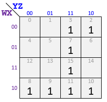
Figure 6.1: K-Map for F(W, X, Y, Z)
- Derive the equation for F from the map. Make sure it is in its simplest form. (No reason to draw a truth table — all the information about the circuit is on the map.)
- Draw the circuit for F. You can draw by hand in your lab journal, but for your lab report, use KiCad and show U-numbers (i.e., U1, U2, etc..). Remember to include "ports" for W, X, Y, Z, and output F. Use only one of each of the following chips: 7408, 7432, and 7404. If you need more, your equation for F is not in its simplest form.
- Suppose your circuit was built and tested with inputs WXYZ from a counter. Let the following table represent oscilloscope waveforms for W and F. The numbers at the top are the 16 states of the counter. The waveform has an error; an incorrect connection was made to one of the AND-gate inputs. Draw the map for F from the waveform, derive F from the map, and compare it with the one you found in a) above. What is the incorrect connection? Show your work and explain your answer.

Exp #6.2 * Build a POS Circuit
This section is like Exp #6.1, except only three inputs will be used: X, Y, Z (from counter outputs QC, QB, QA). You will be assigned a set of 5 numbered squares in an 8-square K-map. Insert a 1 in each square of your set (the other squares contain 0's). Then, derive an equation for F(X, Y, Z) based on your map, as discussed below. As in Exp #6.1, you will need only one each of the following chips: 7408, 7432, and 7404. As a Sum-of-Products (SOP), your equation should have the form
xx + xx + xx
where each "x" represents an input variable, X, Y, or Z, or its complement.
Here is the list of eight sets of numbered squares from which your instructor will choose your set:
01347 12356 21567 30457 40237 50126 61257 70346
The map at the right shows how to fill in the squares for set 30457. From your map, derive an equation for F in the form xx + xx + xx. (Note: you could write F with four xx terms. In this example, you could include both 4-5 and 5-7, but one of them would be redundant. So use only three terms, but make sure you have included all 1's in the map.)
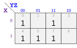
Figure 6.2: K-Map for F(X, Y, Z)

$$F = \overline Y \,\overline Z + X\,\overline Y + Y\,Z$$

$$\eqalign{
& \overline F = \overline X \,\overline Y \,Z + Y\,\overline Z \cr
& \Rightarrow F = \overline F = \overline {\overline X \,\overline Y \,Z + Y\,\overline Z } = (X + Y + \overline Z ) \cdot (\overline Y + Z) \cr} $$
Your instructor should give you a set of numbers squares. If not, you can select a square number based on your team group number:
$TheSquareNumber = \left\{ \matrix{
01347\quad \Rightarrow Group \# = {\rm{\{ 1 \} }} \hfill \cr
12356\quad \Rightarrow Group \# = {\rm{\{ 2 \} }} \hfill \cr
21567\quad \Rightarrow Group \# = {\rm{\{ 3 \} }} \hfill \cr
30457\quad \Rightarrow Group \# = {\rm{\{ 4 \} }} \hfill \cr
40237\quad \Rightarrow Group \# = {\rm{\{ 5 \} }} \hfill \cr
50126\quad \Rightarrow Group \# = {\rm{\{ 6 \} }} \hfill \cr
61257\quad \Rightarrow Group \# = {\rm{\{ 7 \} }} \hfill \cr
70346\quad \Rightarrow Group \# = {\rm{\{ 8 \} }} \hfill \cr} \right.$
- Fill in a map for your set and derive an equation for F in two ways: (You have to simplify the SOP and POS expressions from K-Map shown in Figure 6.2)
YZ 00 01 11 10 X 0 0
1
3
2
1 4
5
7
6
- In SOP form, F = xx + xx + xx, from the 1's of the map.
- In POS (Product-of-Sums) form, F = (x+x+x)(x+x), derive as follows from your map:
- Find the equation for F in the SOP form from the 0's of the map. Do not derive F by complementing your SOP equation for F, since F would then be in POS form, which you do not want.
- Complement F algebraically to get F as a product-of-sums, POS.
- Based on your equations for F, use KiCad to draw two circuits for F: an AND/OR for the SOP form, and an OR/AND for the POS form.
You will need some NOT gates as well for one or both forms of the circuit. - Include both of these circuit diagrams in your lab notebook, but build only the POS one.
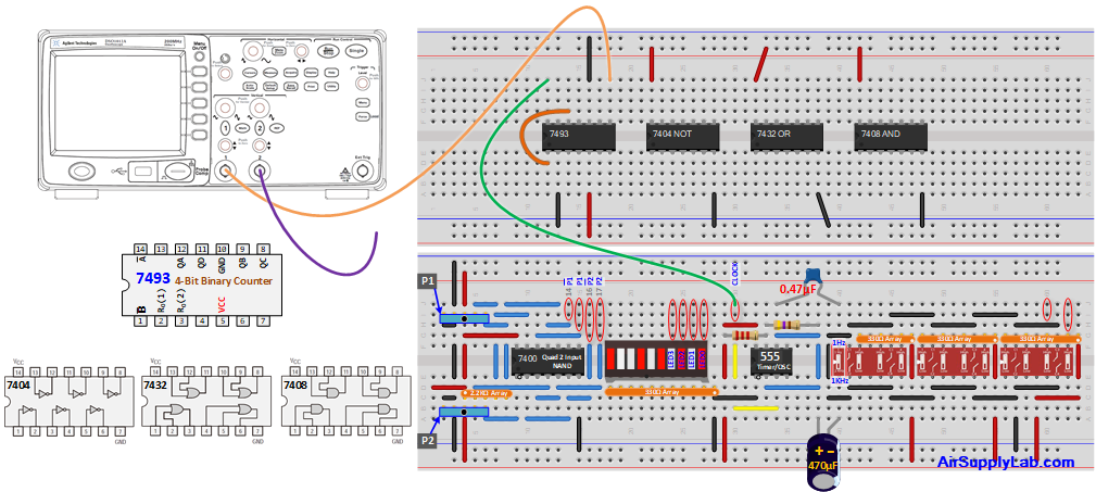
- Test your circuit with counter outputs X, Y, and Z (i.e., QC, QB, and QA). Connect X (or QC) to AIN (channel 1) and F to BIN (channel 2) pin of the ADALM1000/Oscilloscope device (not Y or Z) and capture their waveforms. (Important: trigger-menu settings: since a new cycle of 8 counts begins each time X falls, trigger off the channel that displays X and select negative edge. Adjust the scope's Time mS/Div setting so that one full period of X spans eight divisions on the screen, one per count.)
- Create a map for F from the waveforms and derive an SOP equation for F from the map. Compare it with the SOP equation above from your original map (just as you did in Exp #6.1). If they agree, comment on that fact in your lab notebook. If they do not, debug your circuit to locate the error.
You may be able to do this simply by looking for a difference between the two equations. Suppose your design equation was X Y + Y Z + Y Z. while the one derived from the waveform is X Y + Y Z + Y Z. The error is simply that X was mistakenly connected to an input of the XY gate instead of X.
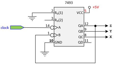
Figure 6.4: The 7493 Count Circuit
Exp #6.2 Circuit Connection for On-Campus Lab
Exp #6.3 ALL NANA/NOR Circuit
All-NAND/NOR Circuits: The goal of a good design is often to minimize the cost and physical size of a circuit. Reducing "chip count" does both, since fewer chips cost less, take up less PC board space, and require less handling (e.g. soldering). Sometimes, chip count can be reduced by designing with all NAND and NOR chips instead of ANDs, ORs, and NOTs (inverters).
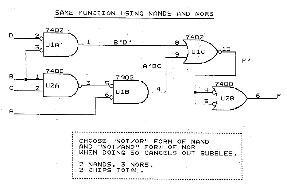
Please refer to the circuit diagram in [Slide 1. SOP Circuit and NAND/NOR Circuit] on the bottom of this Lab. In the left panel of the diagram, the function F = B D + A B C is realized in the usual way using NOTs, ANDs, and ORs. There is a total of 7 gates from 3 chips. The right panel shows the same function realized with all NANDs and NORs. Here, the total is only five gates from 2 chips.
Now, it can be rather complicated to derive the NAND/NOR equivalent algebraically. You would have to operate on F = B D + A B C in several steps:
| 1. | $F = \overline {B + D} + \overline {A + \overline {BC} } $ | OR{NOR (B,D) + NOR[A, NAND(B,C)]} |
| 2. | $\overline F = \overline {\overline {B + D} + \overline {A + \overline {BC} } } $ | NOR{NOR(B,D) + NOR[A, NAND(B,C)} |
| 3. | $F = \overline {\overline {\overline {B + D} + \overline {A + \overline {BC} } } } $ | Complement F with final NOR or NAND (as an inverter). |
The circuit in the right panel of the [Slide 1. SOP Circuit and NAND/NOR Circuit] is the implementation of equation 3.
It is easier (much easier) to skip algebra and work directly on the original circuit. By attaching inversion circles or "bubbles" to the inputs and outputs of AND and OR gates, you can turn them into NANDs and NORs. This graphical method uses alternative (DeMorgan) forms of NANDs and NORs wherever they make it easier to follow circuit logic. Recall DeMorgan's Theorem states:
- (X • Y) = X + Y
- (X + Y) = X • Y
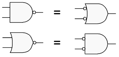
If we think in terms of logic gates, then case (i) means that a NAND gate can be an AND-INVERT (an AND gate with an inverted (bubbled) output) or an INVERT-OR (an OR gate with inverted (bubbled) inputs).
Likewise, case (ii) means that a NOR gate can be an OR-INVERT (an OR gate with an inverted output) or an INVERT-AND (an AND gate with inverted inputs).
Starting from the left diagram in [Slide 1. SOP Circuit and NAND/NOR Circuit], first, reduce the top two inverters to inversion bubbles and attach them to the inputs of the AND. This converts the AND into an invert-AND.
Although this is really a NOR (i.e., a 7402), leave it as an invert-AND so it is easy to see that the output is B D (bottom diagram). Next, reduce the inverter at input A to a bubble and attach it to the input of the following AND. This requires that a bubble be attached to the other AND input as well. Compensate for this by bubbling the output of the AND to its left.
The result is that the left-hand AND becomes an AND-invert (NAND), while the other becomes an invert-AND (a NOR). Finish up by bubbling the output of the OR, which becomes a NOR with output F. Complement this back to F with a final NAND used as an inverter. This NAND is drawn as an invert-OR, so its input bubbles will cancel the bubble of the previous NOR. Note that by showing some gates in their DeMorgan form, you make the logic as easy to follow as in the original NOT-AND-OR circuit. All you have to do is ignore the inversion bubbles when they appear at both ends of a connector. (Note: if NANDs and NORs were all shown in their usual non-DeMorgan forms, it would be hard to understand the underlying simple NOT-AND-OR structure since the effect of the bubbles wouldn't cancel out.)
See Exp #6.4 for more examples that illustrate this.
Additional Uses of NAND/NOR Circuits
In this class, we are using gates built using Transistor-Transistor Logic (TTL) to design our digital circuit. Another logic family commonly used in today's microprocessors, microcontrollers, memory, and other digital circuits is Complementary Metal Oxide Semiconductors (CMOS). CMOS NAND and NOR gates require fewer transistors (switches) than AND and OR gates. Fewer transistors mean smaller integrated circuits, lower power requirements, and lower cost — All desirable features in today's digital systems. This is another important reason for learning how to implement circuits using only NAND and NOR gates.
Exp #6.4 * Draw Diagram
Here you will not build a circuit--only draw its diagram (using KiCad). In Exp #6.2, you chose a function F(X, Y, Z) and designed the circuit using ANDs, ORs, and inverters in SOP and POS form. For this section, convert the SOP (AND/OR) circuit diagram (the one you did not build) into one containing only NAND and NOR gates. (Do not use NOT gates; a NOR or NAND will serve as a NOT if you tie all its inputs together.)
Use DM (DeMorgan) equivalent gate symbols where they are needed, but only then. DM symbols have their inverter bubbles at the front, so use them if their inputs come from gates with bubbled outputs (NORMAL symbols) or from external inputs that are inverted (e.g. X). Otherwise, do not use them. The point is that connecting wires should either have a bubble at each end so the bubbles cancel,![]() , or no bubbles at all (see diagrams in [Slide 1. SOP Circuit and NAND/NOR Circuit],).
, or no bubbles at all (see diagrams in [Slide 1. SOP Circuit and NAND/NOR Circuit],).
Since NANDs are just bubbled ANDs and NORs are just bubbled ORs, your NAND/NOR circuit should resemble the AND/OR design of Exp #6.2, And that is the point; if the connecting wires are bubbled at each end, you can ignore the bubbles and see circuit logic as easily as in Exp#6.2.
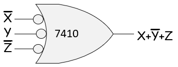
Also, in converting to a NAND/NOR circuit, you might be able to replace two OR gates with a 3-input invert-OR. Example: to produce the OR expression X + Y + Z, use the 3-input NAND (7410) drawn as an inverted OR (notice the inputs have been inverted).
In your lab notebook, include the SOP equation for F and its corresponding circuit diagram from Exp #6.2 as well as the circuit diagram created here. Remember to use DeMorgan gate symbols but only where they are needed. If you use only normal symbols throughout, it will be impossible to follow circuit logic simply by looking at the diagram.
Question
- How many chips (not gates) were required in the circuit of Exp #6.2 compared to the number required here? Did using NANDs and NORs reduce the number of chips?
1. SOP Circuit and NAND/NOR Circuit
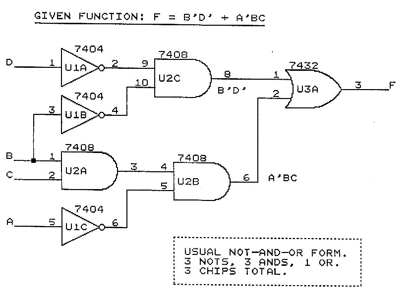
2. Sample Circuit Diagram
