KB 02: DE10-Lite Board
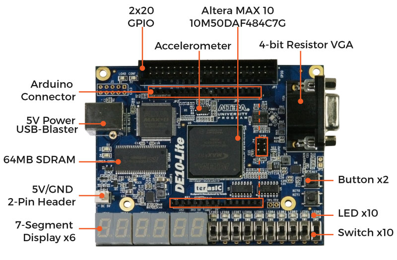
The DE10-List development board includes the following hardware:
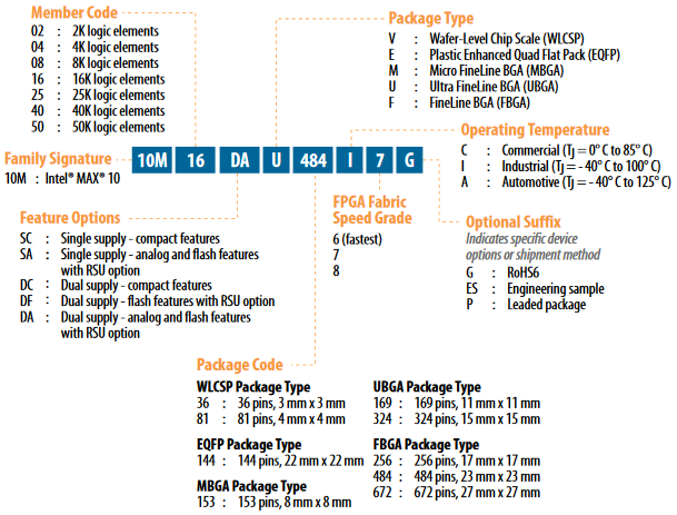
- Intel MAX-10 10M50DAF484C7G FPGA Device
- 50K Programmable Logic Elements
- 1,638 Kbits M9K Memory
- 5,888 Kbit User Flash Memory
- 144 18×18 Multiplier
- 4 PLLs
- On-board USB Blaster
- 3-axis accelerometer
- 4-bit resistor-network DAC for VGA
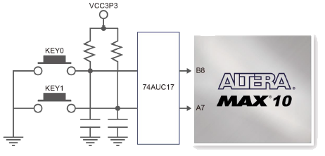
- Two user-defined push-buttons with debounced
- 10 slide switches
- 10 red LEDs
- 6 seven-segment displays
- Arduino Uno R3 compatible connector, including 6 ADC inputs
- 64MB SDRAM, x16 bits data bus
- 2x20 GPIO expansion header
Figure 1 shows the block diagram of the DE10-List board.
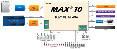
Figure 1: DE10-Lite Board Block Diagram
Status LED
The DE10-Lite development board includes board-specific status LEDs to indicate board status as shown as below.
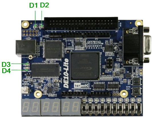
Figure 2: Status LED Position
Table 1: Status LED
| Reference | LED Name | Description |
|---|---|---|
| D1 | LOAD | Illuminates when the onboard USB Blaster is working. |
| D2 | CONF_DONE | Illuminates when the FPGA is successfully configured. |
| D3 | 5V | Illuminates when input power is active. Not installed. |
| D4 | POWER GOOD | Illuminates when the board power system is OK. |
Clock Circuitry
The DE10-Lite board has a 24 MHz oscillator, which is connected to a clock generator, CDCE937. The clock generator is used to distribute clock signals with low jitter and provides the following clock signals to the FPGA board:
- The two 50 MHz clock signals connected to the FPGA are used as clock sources for user logic.
- One 24 MHz clock signal is connected to the clock inputs of the USB microcontroller of USB Blaster.
- One 10 MHz clock signal is connected to the PLL1 and PLL3 of FPGA. The outputs of these two PLLs can drive the ADC clock.
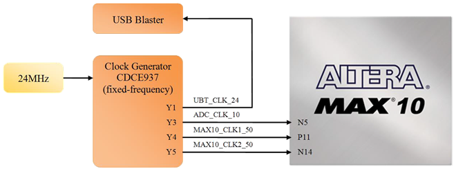
Figure 3: Clock Circuit of the MAX10-Lite Board
Table 2: Pin Assignment of Clock Inputs
| Signal Name | FPGA Pin # | Description | I/O Standard |
|---|---|---|---|
| ADC_CLK_10 | PIN_N5 | 10 MHz clock input for ADC (Bank 3B) | 3.3-V LVTTL |
| MAX10_CLK1_50 | PIN_P11 | 50 MHz clock input (Bank 3B) | 3.3-V LVTTL |
| MAX10_CLK2_50 | PIN_N14 | 50 MHz clock input (Bank 3B) | 3.3-V LVTTL |
Do not modify the clock generator settings. The incorrect setting will cause the system to not work.
User-Defined Slide Switch
There are ten slide switches connected to FPGA on the board. These switches are used as level-sensitive data inputs to a circuit. Each switch is connected directly and individually to a pin on the MAX 10 FPGA.
 When the switch is in the DOWN position (closest to the edge of the board), it provides a low logic level to the FPGA.
 When the switch is in the UP position, it provides a high logic level.
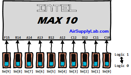
Figure 5: Connections between the slide switches and MAX 10 FPGA
Table 4: Pin Assignment of Slide Switches
| Signal Name | FPGA Pin # | Description | I/O Standard |
|---|---|---|---|
| SW[0] | PIN_C10 | Slide Switch[0] | 3.3-V LVTTL |
| SW[1] | PIN_C11 | Slide Switch[1] | 3.3-V LVTTL |
| SW[2] | PIN_D12 | Slide Switch[2] | 3.3-V LVTTL |
| SW[3] | PIN_C12 | Slide Switch[3] | 3.3-V LVTTL |
| SW[4] | PIN_A12 | Slide Switch[4] | 3.3-V LVTTL |
| SW[5] | PIN_B12 | Slide Switch[5] | 3.3-V LVTTL |
| SW[6] | PIN_A13 | Slide Switch[6] | 3.3-V LVTTL |
| SW[7] | PIN_A14 | Slide Switch[7] | 3.3-V LVTTL |
| SW[8] | PIN_B14 | Slide Switch[8] | 3.3-V LVTTL |
| SW[9] | PIN_F15 | Slide Switch[9] | 3.3-V LVTTL |
User-Defined LEDs
There are ten user-controllable LEDs connected to FPGA on the board. Each LED is driven directly and individually by a pin on the MAX 10 FPGA; driving its associated pin to a high logic level turns the LED on, and driving the pin low turns it off (Positive Logic Outputs).
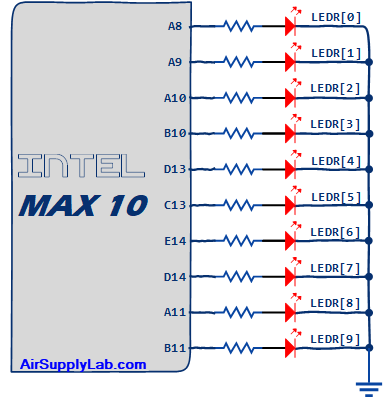
Figure 6: Connections between the LEDs and MAX 10 FPGA
Table 5: Pin Assignment of LEDs
| Signal Name | FPGA Pin # | Description | I/O Standard |
|---|---|---|---|
| LEDR[0] | PIN_A8 | LED [0] | 3.3-V LVTTL |
| LEDR[1] | PIN_A9 | LED [1] | 3.3-V LVTTL |
| LEDR[2] | PIN_A10 | LED [2] | 3.3-V LVTTL |
| LEDR[3] | PIN_B10 | LED [3] | 3.3-V LVTTL |
| LEDR[4] | PIN_D13 | LED [4] | 3.3-V LVTTL |
| LEDR[5] | PIN_C13 | LED [5] | 3.3-V LVTTL |
| LEDR[6] | PIN_E14 | LED [6] | 3.3-V LVTTL |
| LEDR[7] | PIN_D14 | LED [7] | 3.3-V LVTTL |
| LEDR[8] | PIN_A11 | LED [8] | 3.3-V LVTTL |
| LEDR[9] | PIN_B11 | LED [9] | 3.3-V LVTTL |
Seven-Segment Displays
The DE10-Lite board has six 7-segment displays to display numbers. Each seven-segment display consists of seven LED bars, and a single LED round for the decimal point. The DE10-Lite board uses the common anode (CA) method for its displays. This means that all the anodes are tied together and connected to the power source. The segment can be turned ON or OFF by applying a low logic level or high level from the FPGA, respectively (Negative Logic Output). Figure 6 shows the connection of seven segments to pins on MAX 10 FPGA.
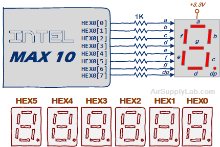
Figure 7: Connections between the 7-Segment Display HEX0 and the MAX 10 FPGA
Table 6: Pin Assignment of 7-Segment Displays
Digit 0
| Signal Name | FPGA Pin # | Description | I/O Standard |
|---|---|---|---|
| HEX0[0] | PIN_C14 | Seven Segment Digit 0:Seg a | 3.3-V LVTTL |
| HEX0[1] | PIN_E15 | Seven Segment Digit 0:Seg b | 3.3-V LVTTL |
| HEX0[2] | PIN_C15 | Seven Segment Digit 0:Seg c | 3.3-V LVTTL |
| HEX0[3] | PIN_C16 | Seven Segment Digit 0:Seg d | 3.3-V LVTTL |
| HEX0[4] | PIN_E16 | Seven Segment Digit 0:Seg e | 3.3-V LVTTL |
| HEX0[5] | PIN_D17 | Seven Segment Digit 0:Seg f | 3.3-V LVTTL |
| HEX0[6] | PIN_C17 | Seven Segment Digit 0:Seg g | 3.3-V LVTTL |
| HEX0[7] | PIN_D15 | Seven Segment Digit 0:Seg dp | 3.3-V LVTTL |
Digit 1
| Signal Name | FPGA Pin # | Description | I/O Standard |
|---|---|---|---|
| HEX1[0] | PIN_C18 | Seven Segment Digit 1:Seg a | 3.3-V LVTTL |
| HEX1[1] | PIN_D18 | Seven Segment Digit 1:Seg b | 3.3-V LVTTL |
| HEX1[2] | PIN_E18 | Seven Segment Digit 1:Seg c | 3.3-V LVTTL |
| HEX1[3] | PIN_B16 | Seven Segment Digit 1:Seg d | 3.3-V LVTTL |
| HEX1[4] | PIN_A17 | Seven Segment Digit 1:Seg e | 3.3-V LVTTL |
| HEX1[5] | PIN_A18 | Seven Segment Digit 1:Seg f | 3.3-V LVTTL |
| HEX1[6] | PIN_B17 | Seven Segment Digit 1:Seg g | 3.3-V LVTTL |
| HEX1[7] | PIN_A16 | Seven Segment Digit 1:Seg dp | 3.3-V LVTTL |
Digit 2
| Signal Name | FPGA Pin # | Description | I/O Standard |
|---|---|---|---|
| HEX2[0] | PIN_B20 | Seven Segment Digit 2:Seg a | 3.3-V LVTTL |
| HEX2[1] | PIN_A20 | Seven Segment Digit 2:Seg b | 3.3-V LVTTL |
| HEX2[2] | PIN_B19 | Seven Segment Digit 2:Seg c | 3.3-V LVTTL |
| HEX2[3] | PIN_A21 | Seven Segment Digit 2:Seg d | 3.3-V LVTTL |
| HEX2[4] | PIN_B21 | Seven Segment Digit 2:Seg e | 3.3-V LVTTL |
| HEX2[5] | PIN_C22 | Seven Segment Digit 2:Seg f | 3.3-V LVTTL |
| HEX2[6] | PIN_B22 | Seven Segment Digit 2:Seg g | 3.3-V LVTTL |
| HEX2[7] | PIN_A19 | Seven Segment Digit 2:Seg dp | 3.3-V LVTTL |
Digit 3
| Signal Name | FPGA Pin # | Description | I/O Standard |
|---|---|---|---|
| HEX3[0] | PIN_F21 | Seven Segment Digit 3:Seg a | 3.3-V LVTTL |
| HEX3[1] | PIN_E22 | Seven Segment Digit 3:Seg b | 3.3-V LVTTL |
| HEX3[2] | PIN_E21 | Seven Segment Digit 3:Seg c | 3.3-V LVTTL |
| HEX3[3] | PIN_C19 | Seven Segment Digit 3:Seg d | 3.3-V LVTTL |
| HEX3[4] | PIN_C20 | Seven Segment Digit 3:Seg e | 3.3-V LVTTL |
| HEX3[5] | PIN_D19 | Seven Segment Digit 3:Seg f | 3.3-V LVTTL |
| HEX3[6] | PIN_E17 | Seven Segment Digit 3:Seg g | 3.3-V LVTTL |
| HEX3[7] | PIN_D22 | Seven Segment Digit 3:Seg dp | 3.3-V LVTTL |
Digit 4
| Signal Name | FPGA Pin # | Description | I/O Standard |
|---|---|---|---|
| HEX4[0] | PIN_F18 | Seven Segment Digit 4:Seg a | 3.3-V LVTTL |
| HEX4[1] | PIN_E20 | Seven Segment Digit 4:Seg b | 3.3-V LVTTL |
| HEX4[2] | PIN_E19 | Seven Segment Digit 4:Seg c | 3.3-V LVTTL |
| HEX4[3] | PIN_J18 | Seven Segment Digit 4:Seg d | 3.3-V LVTTL |
| HEX4[4] | PIN_H19 | Seven Segment Digit 4:Seg e | 3.3-V LVTTL |
| HEX4[5] | PIN_F19 | Seven Segment Digit 4:Seg f | 3.3-V LVTTL |
| HEX4[6] | PIN_F20 | Seven Segment Digit 4:Seg g | 3.3-V LVTTL |
| HEX4[7] | PIN_F17 | Seven Segment Digit 4:Seg dp | 3.3-V LVTTL |
Digit 5
| Signal Name | FPGA Pin # | Description | I/O Standard |
|---|---|---|---|
| HEX5[0] | PIN_J20 | Seven Segment Digit 5:Seg a | 3.3-V LVTTL |
| HEX5[1] | PIN_K20 | Seven Segment Digit 5:Seg b | 3.3-V LVTTL |
| HEX5[2] | PIN_L18 | Seven Segment Digit 5:Seg c | 3.3-V LVTTL |
| HEX5[3] | PIN_N18 | Seven Segment Digit 5:Seg d | 3.3-V LVTTL |
| HEX5[4] | PIN_M20 | Seven Segment Digit 5:Seg e | 3.3-V LVTTL |
| HEX5[5] | PIN_N19 | Seven Segment Digit 5:Seg f | 3.3-V LVTTL |
| HEX5[6] | PIN_N20 | Seven Segment Digit 5:Seg g | 3.3-V LVTTL |
| HEX5[7] | PIN_L19 | Seven Segment Digit 5:Seg dp | 3.3-V LVTTL |
2x20 GPIO Expansion Headers
The DE10-Lite board has one 40-pin expansion header. Each header has 36 user pins connected directly to MAX 10 FPGA. It also comes DV +5V (VCC5), DC+3.3V (VCC3P3), and two GND pins. Both 5V and 3.3V can provide a total of 5W power.
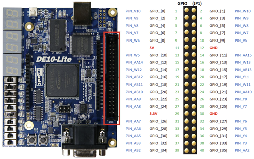
Figure 8: I/O Distribution of the Expansion Headers
Table 7: Pin Assignment of Expansion Headers
Pin 1 — Pin 10
Pin 1 ~ Pin 10
| GPIO Pin # | Signal Name | FPGA Pin # | Description | I/O Standard |
|---|---|---|---|---|
| Pin 1 | GPIO[0] | PIN_V10 | GPIO Connection [0] (Clock_in) | 3.3-V LVTTL |
| Pin 2 | GPIO[1] | PIN_W10 | GPIO Connection [1] | 3.3-V LVTTL |
| Pin 3 | GPIO[2] | PIN_V9 | GPIO Connection [2] (Clock_in) | 3.3-V LVTTL |
| Pin 4 | GPIO[3] | PIN_W9 | GPIO Connection [3] | 3.3-V LVTTL |
| Pin 5 | GPIO[4] | PIN_V8 | GPIO Connection [4] | 3.3-V LVTTL |
| Pin 6 | GPIO[5] | PIN_W8 | GPIO Connection [5] | 3.3-V LVTTL |
| Pin 7 | GPIO[6] | PIN_V7 | GPIO Connection [6] | 3.3-V LVTTL |
| Pin 8 | GPIO[7] | PIN_W7 | GPIO Connection [7] | 3.3-V LVTTL |
| Pin 9 | GPIO[8] | PIN_W6 | GPIO Connection [8] | 3.3-V LVTTL |
| Pin 10 | GPIO[9] | PIN_V5 | GPIO Connection [9] | 3.3-V LVTTL |
Pin 11 — Pin 20
Pin 11 ~ Pin 20
| GPIO Pin # | Signal Name | FPGA Pin # | Description | I/O Standard |
|---|---|---|---|---|
| Pin 11 | + 5V | +5V | ||
| Pin 12 | GND | GND | ||
| Pin 13 | GPIO[10] | PIN_W5 | GPIO Connection [10] | 3.3-V LVTTL |
| Pin 14 | GPIO[11] | PIN_AA15 | GPIO Connection [11] | 3.3-V LVTTL |
| Pin 15 | GPIO[12] | PIN_AA14 | GPIO Connection [12] | 3.3-V LVTTL |
| Pin 16 | GPIO[13] | PIN_W13 | GPIO Connection [13] | 3.3-V LVTTL |
| Pin 17 | GPIO[14] | PIN_W12 | GPIO Connection [14] | 3.3-V LVTTL |
| Pin 18 | GPIO[15] | PIN_AB13 | GPIO Connection [15] | 3.3-V LVTTL |
| Pin 19 | GPIO[16] | PIN_AB12 | GPIO Connection [16] | 3.3-V LVTTL |
| Pin 20 | GPIO[17] | PIN_Y11 | GPIO Connection [17] | 3.3-V LVTTL |
Pin 21 — Pin 30
Pin 21 ~ Pin 30
| GPIO Pin # | Signal Name | FPGA Pin # | Description | I/O Standard |
|---|---|---|---|---|
| Pin 21 | GPIO[18] | PIN_AB11 | GPIO Connection [18] | 3.3-V LVTTL |
| Pin 22 | GPIO[19] | PIN_W11 | GPIO Connection [19] | 3.3-V LVTTL |
| Pin 23 | GPIO[20] | PIN_AB10 | GPIO Connection [20] | 3.3-V LVTTL |
| Pin 24 | GPIO[21] | PIN_AA10 | GPIO Connection [21] | 3.3-V LVTTL |
| Pin 25 | GPIO[22] | PIN_AA9 | GPIO Connection [22] | 3.3-V LVTTL |
| Pin 26 | GPIO[23] | PIN_Y8 | GPIO Connection [23] | 3.3-V LVTTL |
| Pin 27 | GPIO[24] | PIN_AA8 | GPIO Connection [24] | 3.3-V LVTTL |
| Pin 28 | GPIO[25] | PIN_Y7 | GPIO Connection [25] | 3.3-V LVTTL |
| Pin 29 | +3.3V | +3.3V | ||
| Pin 30 | GND | GND |
Pin 31 — Pin 40
Pin 31 ~ Pin 40
| GPIO Pin # | Signal Name | FPGA Pin # | Description | I/O Standard |
|---|---|---|---|---|
| Pin 31 | GPIO[26] | PIN_AA7 | GPIO Connection [26] | 3.3-V LVTTL |
| Pin 32 | GPIO[27] | PIN_Y6 | GPIO Connection [27] | 3.3-V LVTTL |
| Pin 33 | GPIO[28] | PIN_AA6 | GPIO Connection [28] | 3.3-V LVTTL |
| Pin 34 | GPIO[29] | PIN_Y5 | GPIO Connection [29] | 3.3-V LVTTL |
| Pin 35 | GPIO[30] | PIN_AA5 | GPIO Connection [30] | 3.3-V LVTTL |
| Pin 36 | GPIO[31] | PIN_Y4 | GPIO Connection [31] | 3.3-V LVTTL |
| Pin 37 | GPIO[32] | PIN_AB3 | GPIO Connection [32] | 3.3-V LVTTL |
| Pin 38 | GPIO[33] | PIN_Y3 | GPIO Connection [33] | 3.3-V LVTTL |
| Pin 39 | GPIO[34] | PIN_AB2 | GPIO Connection [34] | 3.3-V LVTTL |
| Pin 40 | GPIO[35] | PIN_AA2 | GPIO Connection [35] | 3.3-V LVTTL |
Arduino Uno R3 Expansion Header
The DE10-Lite board also provides an Arduino Uno revision 3 compatibility expansion header, which comes with four independent headers. The expansion header has 17 user pins: included 16 pin2 GPIO and 1 pin Reset) connected directly to the MAX 10 FPGA. 6-pin Analog input connects to ADC and provides DC +5V (VCC5), DC +3.3V (VCC3P3 and IOREF), and three GND pins.
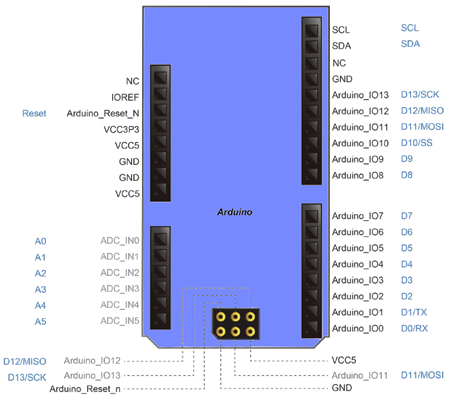
Figure 9: Pin Out Signals Name of the Arduino Uno Connector. (The Blue Font Represents the Arduino Pin-Out Definition)
Digital I/O Pins
The 16 GPIO pins are provided to the Arduino Header for digital I/O.
Table 8: Pin Assignment of Arduino Uno Expansion Header Connector
| Signal Name | FPGA Pin # | Description | I/O Standard |
|---|---|---|---|
| ARDUINO_IO[0] | PIN_AB5 | Arduino I/O: D0/RX | 3.3-V LVTTL |
| ARDUINO_IO[1] | PIN_AB6 | Arduino I/O: D1/TX | 3.3-V LVTTL |
| ARDUINO_IO[2] | PIN_AB7 | Arduino I/O: D2 | 3.3-V LVTTL |
| ARDUINO_IO[3] | PIN_AB8 | Arduino I/O: D3 | 3.3-V LVTTL |
| ARDUINO_IO[4] | PIN_AB9 | Arduino I/O: D4 | 3.3-V LVTTL |
| ARDUINO_IO[5] | PIN_Y10 | Arduino I/O: D5 | 3.3-V LVTTL |
| ARDUINO_IO[6] | PIN_AA11 | Arduino I/O: D6 | 3.3-V LVTTL |
| ARDUINO_IO[7] | PIN_AA12 | Arduino I/O: D7 | 3.3-V LVTTL |
| ARDUINO_IO[8] | PIN_AB17 | Arduino I/O: D8 | 3.3-V LVTTL |
| ARDUINO_IO[9] | PIN_AA17 | Arduino I/O: D9 | 3.3-V LVTTL |
| ARDUINO_IO[10] | PIN_AB19 | Arduino I/O: D10/SS | 3.3-V LVTTL |
| ARDUINO_IO[11] | PIN_AA19 | Arduino I/O: D11/MOSI | 3.3-V LVTTL |
| ARDUINO_IO[12] | PIN_Y19 | Arduino I/O: D12/MISO | 3.3-V LVTTL |
| ARDUINO_IO[13] | PIN_AB20 | Arduino I/O: D13/SCK | 3.3-V LVTTL |
| ARDUINO_IO[14] | PIN_AB21 | Arduino I/O: SDA | 3.3-V LVTTL |
| ARDUINO_IO[15] | PIN_AA20 | Arduino I/O: SCL | 3.3-V LVTTL |
| ARDUINO_RESET_N | PIN_F16 | Arduino I/O: /Reset (Low Active) | 3.3-V Schmitt Trigger |
Analog Pins
Besides 16 pins for digital GPIO, there are also 6 analog inputs on the Arduino Uno R3 Expansion Header (A0 ~ A5). Consequently, we use MAX 10 FPGA ADC on the board for possible future analog-to-digital applications. We will introduce it in the next tab.
Table 9: Pin Assignment of Arduino Uno Expansion Analog Header Connector
| Signal Name | FPGA Pin # | Description | I/O Standard |
|---|---|---|---|
| ADC1IN1 | PIN_F5 | Arduino I/O: A0 | 3.3-V LVTTL |
| ADC1IN2 | PIN_F4 | Arduino I/O: A1 | 3.3-V LVTTL |
| ADC1IN3 | PIN_J8 | Arduino I/O: A2 | 3.3-V LVTTL |
| ADC1IN4 | PIN_J9 | Arduino I/O: A3 | 3.3-V LVTTL |
| ADC1IN5 | PIN_H3 | Arduino I/O: A4 | 3.3-V LVTTL |
| ADC1IN6 | PIN_J4 | Arduino I/O: A5 | 3.3-V LVTTL |
ADC Converter and Analog Input
The MAX 10 FPGA has two ADC channels: ADC1 and ADC2. On the DE10-Lite board, only ADC1 is brought out to pins, and there is no access to ADC2 inputs. The ADC configurations on MAX 10 FPGA are shown as below:
- 2 ADC channels
- SAR type conversion
- 12-bit conversion
- 1MHz (max) operation
- 1 dedicated input/channel
- 8 programmable inputs/channel
- 0 ~ 2.5V conversion range Arduino analog pins (A0 ~ A5) are mapped to ADC1IN1 ~ ADC1IN6.
The DE10-Lite board has eight analog inputs that are connected to MAX 10 FPGA ADC1 through a 1x6 and a 1x2 header input, wherein the 1x2 header is reserved and not mounted with parts.
All analog input signals that are sourced through the Arduino header JP8 are first filtered by the Analog Front-End circuit. This circuit scales the maximum allowable voltage per the Arduino specification (5.0V) to the maximum allowable voltage per the MAX 10 FPGA ADC IP block (2.5V).

Figure 10: The Analog Front-End Circuit between the Arduino Analog Input and MAX 10 FPGA
The 12-bit of ADC value represents 0 ~ 2.5V input voltage to the ADC hardware. In the ADC front-end circuit, the output voltage is half of the input voltage. So the input voltage to the Arduino analog input can be calculated with the formula listed below:
$$Vol {_{input}} = {{AD{C_{12 - bit}}} \over {4096}} \times 2.5 \times 2 = {{AD{C_{12 - bit}}} \over {4096}} \times 5\quad (V)$$
Table 10: Pin Assignment of ADC
| Signal Name | FPGA Pin # | Description | I/O Standard |
|---|---|---|---|
| ADC1IN1 | PIN_F5 | Arduino I/O: A0 (ADC_IN0) | 3.3-V LVTTL |
| ADC1IN2 | PIN_F4 | Arduino I/O: A1 (ADC_IN1) | 3.3-V LVTTL |
| ADC1IN3 | PIN_J8 | Arduino I/O: A2 (ADC_IN2) | 3.3-V LVTTL |
| ADC1IN4 | PIN_J9 | Arduino I/O: A3 (ADC_IN3) | 3.3-V LVTTL |
| ADC1IN5 | PIN_H3 | Arduino I/O: A4 (ADC_IN4) | 3.3-V LVTTL |
| ADC1IN6 | PIN_J4 | Arduino I/O: A5 (ADC_IN5) | 3.3-V LVTTL |
| ADC1IN7 | PIN_K5 | TP1 (ADC_IN6) | 3.3-V LVTTL |
| ADC1IN8 | PIN_K6 | TP2 (ADC_IN7) | 3.3-V LVTTL |
VGA
The DE10-Lite board includes a 15-pin D-SUB connector for VGA output. The VGA synchronization signals are provided directly from the MAX 10 FPGA, and a 4-bit DAC using resistor-network is used to produce the analog data signals (red, green, and blue). The associated schematic is given in Figure 11 and can support standard VGA resolution (640x480 pixels, at 25 MHz).
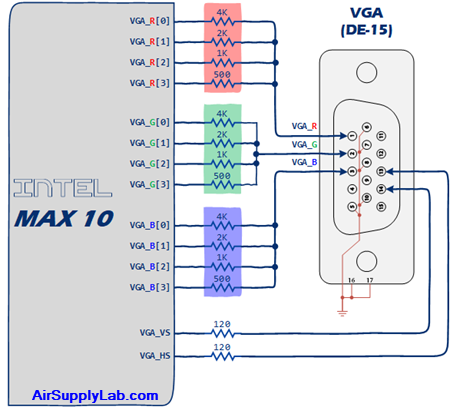
Figure 11: Connections Between the VGA and MAX 10 FPGA
Table 11: Pin Assignment of VGA
| Signal Name | FPGA Pin # | Description | I/O Standard |
|---|---|---|---|
| VGA_R[0] | PIN_AA1 | VGA Red [0] | 3.3-V LVTTL |
| VGA_R[1] | PIN_V1 | VGA Red [1] | 3.3-V LVTTL |
| VGA_R[2] | PIN_Y2 | VGA Red [2] | 3.3-V LVTTL |
| VGA_R[3] | PIN_Y1 | VGA Red [3] | 3.3-V LVTTL |
| VGA_G[0] | PIN_W1 | VGA Green [0] | 3.3-V LVTTL |
| VGA_G[1] | PIN_T2 | VGA Green [1] | 3.3-V LVTTL |
| VGA_G[2] | PIN_R2 | VGA Green [2] | 3.3-V LVTTL |
| VGA_G[3] | PIN_R1 | VGA Green [3] | 3.3-V LVTTL |
| VGA_B[0] | PIN_P1 | VGA Blue [0] | 3.3-V LVTTL |
| VGA_B[1] | PIN_T1 | VGA Blue [1] | 3.3-V LVTTL |
| VGA_B[2] | PIN_P4 | VGA Blue [2] | 3.3-V LVTTL |
| VGA_B[3] | PIN_N2 | VGA Blue [3] | 3.3-V LVTTL |
| VGA_HS | PIN_N3 | VGA Horizontal Sync | 3.3-V LVTTL |
| VGA_VS | PIN_N1 | VGA Vertical Sync | 3.3-V LVTTL |
SDRAM
The board features 64MB of SDRAM with a single 64MB (32Mx16) SDRAM chip. The chip consists of a 16-bit data line, control line, and address line connected to the FPGA. This chip uses the 3.3V LVCMOS signaling standard. Connections
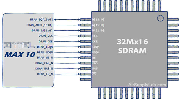
Figure 12: Connections between the SDRAM and MAX 10 FPGA
Table 12: Pin Assignment of SDRAM
Address Bus
| Signal Name | FPGA Pin # | Description | I/O Standard |
|---|---|---|---|
| DRAM_ADDR[0] | PIN_U17 | SDRAM Address[0] | 3.3-V LVTTL |
| DRAM_ADDR[1] | PIN_W19 | SDRAM Address[1] | 3.3-V LVTTL |
| DRAM_ADDR[2] | PIN_V18 | SDRAM Address[2] | 3.3-V LVTTL |
| DRAM_ADDR[3] | PIN_U18 | SDRAM Address[3] | 3.3-V LVTTL |
| DRAM_ADDR[4] | PIN_U19 | SDRAM Address[4] | 3.3-V LVTTL |
| DRAM_ADDR[5] | PIN_T18 | SDRAM Address[5] | 3.3-V LVTTL |
| DRAM_ADDR[6] | PIN_T19 | SDRAM Address[6] | 3.3-V LVTTL |
| DRAM_ADDR[7] | PIN_R18 | SDRAM Address[7] | 3.3-V LVTTL |
| DRAM_ADDR[8] | PIN_P18 | SDRAM Address[8] | 3.3-V LVTTL |
| DRAM_ADDR[9] | PIN_P19 | SDRAM Address[9] | 3.3-V LVTTL |
| DRAM_ADDR[10] | PIN_T20 | SDRAM Address[10] | 3.3-V LVTTL |
| DRAM_ADDR[11] | PIN_P20 | SDRAM Address[11] | 3.3-V LVTTL |
| DRAM_ADDR[12] | PIN_R20 | SDRAM Address[12] | 3.3-V LVTTL |
Data Bus
| Signal Name | FPGA Pin # | Description | I/O Standard |
|---|---|---|---|
| DRAM_DQ[0] | PIN_Y21 | SDRAM Data[0] | 3.3-V LVTTL |
| DRAM_DQ[1] | PIN_Y20 | SDRAM Data[1] | 3.3-V LVTTL |
| DRAM_DQ[2] | PIN_AA22 | SDRAM Data[2] | 3.3-V LVTTL |
| DRAM_DQ[3] | PIN_AA21 | SDRAM Data[3] | 3.3-V LVTTL |
| DRAM_DQ[4] | PIN_Y22 | SDRAM Data[4] | 3.3-V LVTTL |
| DRAM_DQ[5] | PIN_W22 | SDRAM Data[5] | 3.3-V LVTTL |
| DRAM_DQ[6] | PIN_W20 | SDRAM Data[6] | 3.3-V LVTTL |
| DRAM_DQ[7] | PIN_V21 | SDRAM Data[7] | 3.3-V LVTTL |
| DRAM_DQ[8] | PIN_P21 | SDRAM Data[8] | 3.3-V LVTTL |
| DRAM_DQ[9] | PIN_J22 | SDRAM Data[9] | 3.3-V LVTTL |
| DRAM_DQ[10] | PIN_H21 | SDRAM Data[10] | 3.3-V LVTTL |
| DRAM_DQ[11] | PIN_H22 | SDRAM Data[11] | 3.3-V LVTTL |
| DRAM_DQ[12] | PIN_G22 | SDRAM Data[12] | 3.3-V LVTTL |
| DRAM_DQ[13] | PIN_G20 | SDRAM Data[13] | 3.3-V LVTTL |
| DRAM_DQ[14] | PIN_G19 | SDRAM Data[14] | 3.3-V LVTTL |
| DRAM_DQ[15] | PIN_F22 | SDRAM Data[15] | 3.3-V LVTTL |
Control Bus
| Signal Name | FPGA Pin # | Description | I/O Standard |
|---|---|---|---|
| DRAM_BA[0] | PIN_T21 | SDRAM Bank Address[0] | 3.3-V LVTTL |
| DRAM_BA{1] | PIN_T22 | SDRAM Bank Address[1] | 3.3-V LVTTL |
| DRAM_LDQM | PIN_V22 | SDRAM byte Data Mask [0] | 3.3-V LVTTL |
| DRAM_UDQM | PIN_J21 | SDRAM byte Data Mask [1] | 3.3-V LVTTL |
| DRAM_RAS_N | PIN_U22 | SDRAM Row Address Strobe | 3.3-V LVTTL |
| DRAM_CAS_N | PIN_U21 | SDRAM Column Address Strobe | 3.3-V LVTTL |
| DRAM_CKE | PIN_N22 | SDRAM Clock Enable | 3.3-V LVTTL |
| DRAM_CLK | PIN_L15 | SDRAM Clock | 3.3-V LVTTL |
| DRAM_WE_N | PIN_V20 | SDRAM Write Enable | 3.3-V LVTTL |
| DRAM_CS_N | PIN_U20 | SDRAM Chip Select | 3.3-V LVTTL |
Accelerometer Sensor
The board comes with a digital accelerometer sensor module (ADXL345), commonly known as G-sensor. This G-sensor is a small, thin, ultralow-power assumption 3-axis accelerometer with high-resolution measurement. Digitalized output is formatted as 16-bit in two’s complement and can be accessed through SPI (3- and 4-wire) and I2C digital interfaces.
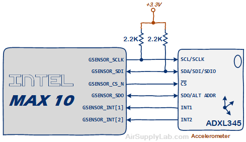
Figure 13: The Connections between the Accelerometer Sensor and MAX 10 FPGA.
Table 13: Pin Assignment of Accelerometer Sensor
| Signal Name | FPGA Pin # | Description | I/O Standard |
|---|---|---|---|
| GSENSOR_SDI | PIN_V11 | I2C Serial Data SPI MOSI (SPI 4-wire) SPI SDAT (SPI 3-wire) |
3.3-V LVTTL |
| GSENSOR_SDO | PIN_V12 | SPI MISO (SPI 4-wire) Alternate I2C Address Select |
3.3-V LVTTL |
| GSENSOR_CS_N | PIN_AB16 | I2C/SPI Mode Selection: 1: SPI Idle Mode / I2C Communication Enabled 0: SPI Communication Mode / I2C Disabled SPI Chip Select |
3.3-V LVTTL |
| GSENSOR_SCLK | PIN_AB15 | I2C Serial Clock SPI Serial Clock (3- and 4-wire) |
3.3-V LVTTL |
| GSENSOR_INT[1] | PIN_Y14 | Interrupt Pin1 | 3.3-V LVTTL |
| GSENSOR_INT[2] | PIN_Y13 | Interrupt Pin2 | 3.3-V LVTTL |
I2C Mode
I2C Mode
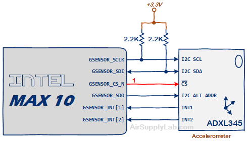
If the CS pin is tied high to VDD (logic 1), the ADXL345 will operate in I2C slave mode. The I2C address is configured by the GSENSOR_SDO pin, and the address values are shown below.
| Signal Name | Setting | Description |
|---|---|---|
| GSENSOR_SDI | I2C DAT | I2C Serial Data |
| GSENSOR_SDO | Address | 0: I2C Address = 0x53 1: I2C Address = 0x1D |
| GSENSOR_CS_N | 1 | I2C Mode |
| GSENSOR_SCLK | I2C CLK | I2C Clock |
SPI (4-Wire) Mode
SPI (4-Wire) Mode
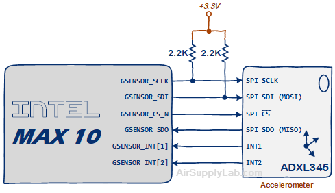
The ADXL345 can be configured in either 3- or 4- wire SPI mode. Clearing the SPI bit (Bit 6) in the DATA_FORMAT register (Register Address 0x31) selects the 4-wire mode. The maximum SPI clock speed is 5MHz with 100 pF maximum loading, and the timing scheme follows clock polarity (CPOL) = 1 and clock phase (CPHA) = 1.
| Signal Name | Setting | Description |
|---|---|---|
| GSENSOR_SDI | SPI SDI | SPI Serial Data Input (MOSI) |
| GSENSOR_SDO | SPI SDO | SPI Serial Data Output (MISO) |
| GSENSOR_CS_N | SPI CS | SPI Chip Select |
| GSENSOR_SCLK | SPI SCLK | SPI Serial Clock |
SPI (3-Wire) Mode
SPI (3-Wire) Mode
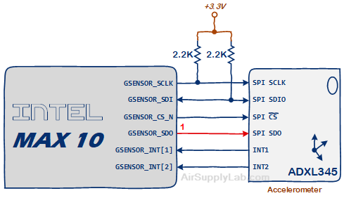
The ADXL345 can be configured in either 3- or 4- wire SPI mode. Setting the SPI bit (Bit 6) in the DATA_FORMAT register (Register Address 0x31) selects the 3-wire mode. The maximum SPI clock speed is 5MHz with 100 pF maximum loading, and the timing scheme follows clock polarity (CPOL) = 1 and clock phase (CPHA) = 1.
| Signal Name | Setting | Description |
|---|---|---|
| GSENSOR_SDI | SPI SDIO | SPI Serial Data Input and Output |
| GSENSOR_SDO | 1 | Not Used |
| GSENSOR_CS_N | SPI CS | SPI Chip Select |
| GSENSOR_SCLK | SPI SCLK | SPI Serial Clock |
Boot Selection
The DE10-Lite board supports the dual image boot function. If you want to use this function, you will need to solder the JP5 with a 2-pin header (pitch 0.1" = 0.25mm) by yourself.
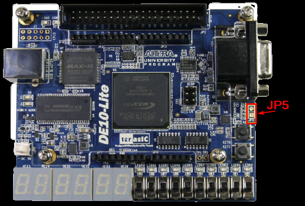
Figure 14: JP5 Position on the DE10-List Board.
Table 14: JP5 Jumper Setting Instructions
| Reference | Jumper Setting | Description |
|---|---|---|
| JP5 | Open (Default) | Boot from image 0 |
| Close | Boot from image 1 |
MAX10 Device Resources
| Resources | Device | |||||||
|---|---|---|---|---|---|---|---|---|
| 10M02 | 10M04 | 10M08 | 10M16 | 10M25 | 10M40 | 10M50 | ||
| Logic Elements (LE) (K) | 2 | 4 | 8 | 16 | 25 | 40 | 50 | |
| M9K Memory (Kb) | 108 | 189 | 378 | 549 | 675 | 1,260 | 1,638 | |
| User Flash Memory (Kb) | 96 | 1,248 | 1,376 | 2,368 | 3,200 | 5,888 | 5,888 | |
| 18 × 18 Multiplier | 16 | 20 | 24 | 45 | 55 | 125 | 144 | |
| PLL | 2 | 2 | 2 | 4 | 4 | 4 | 4 | |
| GPIO | 246 | 246 | 250 | 320 | 360 | 500 | 500 | |
| LVDS | Dedicated Transmitter |
15 | 15 | 15 | 22 | 24 | 30 | 30 |
| Emulated Transmitter |
114 | 114 | 116 | 151 | 171 | 241 | 241 | |
| Dedicated Receiver | 114 | 114 | 116 | 151 | 171 | 241 | 241 | |
| Internal Configuration Image | 1 | 2 | 2 | 2 | 2 | 2 | 2 | |
| ADC | — | 1 | 1 | 1 | 2 | 2 | 2 | |
