Lab 01: Introduction to Electrical Circuits
Objective
- Understand the fundamental concepts of voltage, current, and resistance.
- Learn how transistors function as electrical switches.
- Study the role of transistors in logic gates.
- Apply Ohm's Law to simple electrical circuits.
- Explore the use of LEDs and resistors in circuits.
- Build and analyze a simple NOT gate using transistors.
Required Reading Materials
- Breadboard
- Resistor Color Code: EE3450-Tiva Lab ASM 12: Calling Assembly Functions from C
- Lesson 07: Logical Functions and Selection Structures
- Online Digilent Analog Discovery 2 Reference Manual or pdf
- Online WaveForms Reference Manual or pdf
- How LED Works: https://www.explainthatstuff.com/diodes.html
Components Required
| Component/Device | Description | Quantity |
|---|---|---|
| 15 KΩ (brn grn orn gld) | × 1 | |
| 2.2 KΩ (red red red gld) | × 1 | |
| 330 Ω (orn orn brn gld) | × 1 | |
| Green LED | × 1 | |
| 2N4124 NPN Transistor | × 1 | |
| Pushbutton Switch | × 1 |
Background
Electrical Circuits
Simply defined, an electric circuit is a closed-loop where through which charges (electrons) can continually flow. Electric circuits can be analog or digital.
- Analog circuits operate on continuous signals.
- Digital circuits operate on discrete, usually binary, signals.
Binary signals have two discrete values or logic levels:- Logic 1: A high value of voltage (5V) in this lab
- Logic 0: A low value (0V or ground)
Fundamental components in analog circuits are Resistors, capacitors, inductors, diodes, transistors, and operational amplifiers. Fundamental components in digital circuits are transistors, logic gates, and integrated circuits (ICs). The ICs are a combination of logic gates that are integrated to implement simple digital circuits like counters and decoders and more complex digital systems like microprocessors and microcontrollers. As you'll discover in this experiment, all the digital components are actually analog circuits underneath.
Many circuits will have both analog and digital components such as in embedded systems which may have analog inputs such as sensors and analog outputs such as output voltages that control motor speed and a digital microcontroller programmed to control the system.
In this experiment, you will be introduced to the basics of voltage, current, and resistance which are the building blocks of any electric circuit. You will also discover how transistors work as electrical switches and see how they can be combined to build digital components known as logic gates.
Ohm's Law
Electricity is the movement and interaction of electrons which are charged particles. Voltage is a measure of the potential difference in charge between two points in an electric field. Voltage is measured in volts (V) which is a measure of the energy per unit charge. So a battery that is a source of energy (electrons) will have a potential difference in charge between its two terminals. For example, a 9V battery would supply 9 Joules of electric potential energy per every 1 Coulomb of charge which moves between its negative and positive terminals. Current, measured in amperes (A), is the rate at which electric charge flows past a point in a circuit. When a load is connected to the positive and negative terminals of a battery, an electric circuit will be formed, and current will flow within the battery from its negative terminal to its positive terminal, then through the load and back to the negative terminal. A load in a circuit is an electrical component containing resistance, which dissipates energy as heat; examples are the appliances and lights in your home. Resistance is measured in Ohms (Ω). Ohm's Law defines the relationship between voltage, current, and resistance.
$V = IR$
Here $V$ represents the voltage, $I$ represents the current, and $R$ represents the resistance.
While all electrical components, including wires, have some level of resistance, Resistors are manufactured components with specific ohmic values designed to control the amount of current flowing through a circuit. They are passive components that consume power. Resistors have two terminals (end-points) and are represented by a zig-zag line such as:
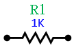
Here R1 refers to a specific resistor in a circuit, and 1K is an abbreviation of 1 KΩ (or 1x10³ Ohms) which is the value of the resistor. Resistors are manufactured to provide various values of resistance and, as mentioned earlier, are color-coded to indicate those values.
Experiments
Every experiment section that requires you to build a circuit and test it has an asterisk (*). For those sections:
- For the in-class lab: Demonstrate the working circuit to your lab instructor.
- For online lab: Take a video to describe your circuit, upload the video to YouTube, and put the link in the report.
Exp #1.1 Simple Circuit with DC Power and a Resistor
Figure 1.1 below shows a simple electric circuit with a power source (voltage supply) and a resistor connected together using wires. The power source provides electric energy to the load, which is this case is the resistor. The power source could be a battery or a power supply such as the adjustable DC (direct current) power supply that we will be using in this lab. The power supply converts AC (alternating current) voltage from the wall outlet to an adjustable DC voltage.
The energy for the AC power source could come from many different sources including wind, solar, fossil fuels (coal, oil, natural gas), hydrogen, hydroelectric (water), and nuclear. The DC power supply is regulated to provide a constant voltage or current. In our lab, we will be using TTL (Transistor-Transistor-Logic) chips which typically use a 5V voltage supply. TTL logic treats input voltage levels in the range 0V to 0.8V as logic zero and levels in the range 2V to 5V as logic one.
In the circuit of Figure 1.1, current ($I$) flows through the resistor as shown. To determine how much current will flow, we can use Ohm's Law.
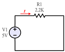
Figure 1.1: Simple Electric Circuit with Power Supply (V1) and Resistor (R1)
Question
- Use Ohm's Law to compute the current in the circuit of Figure 1.1. Place your calculation steps and results in your lab journal.
Exp #1.2 * Simple Circuit with a Resistor and LED
Part A
You could build the circuit in Figure 1.1 and confirm your computation by measuring the current using a multimeter (you will do this type of measurement in your EE 2049 lab). For this course, we just want to gain a basic understanding of electric circuits before delving into digital logic circuits. Rather than measure the current, we want to observe the effect of varying the resistance on another load, namely an LED (Light-Emitting Diode).
A diode is an electrical component built from a semiconductor material that only allows current to flow through it in one direction. In an LED, when the current flows through the diode, light is emitted. LEDs are designed to emit light of a specific wavelength (color) depending on the material that the LED is made from. LEDs are non-ohmic devices (they do not follow Ohm's Law). There will be a voltage drop (called the forward bias voltage) across the LED when it is on. The voltage drop is dependent on what wavelength the LED is designed to emit (e.g., the color of the LED). For the green LED we are using in this experiment, we will assume the voltage drop is 2.1V.
Figure 1.2 (below) shows a circuit diagram with a resistor and LED. Resistors are used to control the amount of current flowing through the LED. If the circuit were connected without the resistor, the LED would be over-driven; it would light brightly for a while and then burn out.
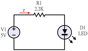
Figure 1.2: Simple Electric Circuit with Resistor and LED
In Figure 1.1, the voltage across the resistor was equal to the full supply voltage (ignoring any voltage drops due to the resistance in the wires) so VR = 5V. But in Figure 1.2, the 5V is divided between R1 and the LED. Assuming a 2.1V drop across the LED, the voltage across the resistor is thus $VR = 5V – 2.1V = 2.9V$. For this circuit, compute the current flow I around the loop.
Question
- Draw three circuits as in Figure 1.2 with a different resistor (2.2KΩ, 330Ω, and 15KΩ) in your lab report. Calculator the value of current for the 2.2KΩ resistor, a 330Ω, and a 15KΩ resistor. Show all calculations.
- Assuming that the maximum current through the LED is 20mA and the voltage drop across the LED is 2.1V, compute the smallest value for R1 that can be used without damaging the LED. Include the question and your answer in your lab report.
Part B * (* Lab Work)
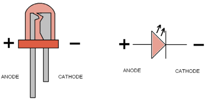
Figure 1.3: LED Terminals
The anode (+) terminal has the longer lead and the cathode (-) terminal has the short lead
Build the circuit shown in Figure 1.2 on the breadboard. While the orientation of a resistor in a circuit does not matter (current can flow in either direction through a resistor), current can only flow in one direction in an LED, from the anode (positive terminal) to the cathode (negative terminal). Figure 1.3 shows how to determine which is the anode (longer lead/wire) and which is the cathode (shorter lead). Figure 1.4 (below) shows how to connect the components.
Exp #1.2(B) Circuit Connection for On-Campus Lab
Note that on your breadboard, the five holes along each row are internally connected. Also, note that there are two buses running vertically along each section of the board. The red bus has been wired to connect to the positive terminal of the breadboard, which, in turn, is connected to the positive terminal of the power supply (5V). Similarly, the blue bus has been wired to connect to the negative terminal of the breadboard which, in turn, is connected to the ground terminal of the power supply (0V).
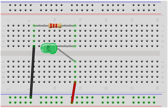
Figure 1.4: Example of how to build the circuit from Figure 1.2 on your breadboard.
First, turn on the power supply and adjust the supply output voltage to 5V. Then, wire up your circuit and connect the negative (ground) terminal of the DC power supply to the breadboard's negative terminal's banana "jack" (opposite of the banana plug). Likewise, connect the positive terminal of the power supply to the breadboard's positive terminal's jack.
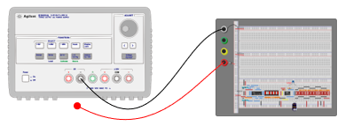
Figure 1.4 (b): Turn on the power supply, set the output voltage to 5V, then connect the power source to the breadboard.
Question
- Connect vary the values of R1 on the breadboard, observe the brightness of the LED, and take a picture of each. Fill in Table 1.3 and enter it in your journal. Post the pictures and describe the observations in a paragraph in the report.
R1-Value Observations on LED Brightness
(dark, dim, bright, brightest)2.2 KΩ 330 Ω 15 KΩ - What is the relationship between the amount of current flowing through the LED and the brightness of the LED?
- Connect a 330Ω as R1 in your circuit. Change the supply voltage from 5V to 0V and record your observations. At what voltage level does the LED seem to turn off? (If you use the ADALM1000 device, you can skip this question)
Exp #1.3* Switch
Oftentimes circuits are controlled by a switch. Think about the lights and appliances in your house. In the circuit that you built in the previous section (Figure 1.4), you could manually turn the LED off by removing one of the circuit's wires to create an open circuit (current cannot flow through an open circuit) and then replacing it to close the circuit and turn the LED on. Creating an open or closed circuit using a switch is far more efficient.
Exp #1.3 Circuit Connection for On-Campus Lab
Figure 1.5 shows an example of a pushbutton switch different from the ones in the test circuit. This one has 3 leads. When the switch is not depressed (normal condition) the center lead is internally connected to the right-hand lead (the upper contact). When the button is depressed, the center lead connects to the left-hand lead (the lower contact). We can use this to control the circuit in Fig. 1-6 as described below.
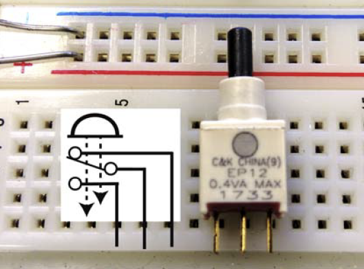
Figure 1.5: The Pushbutton Switch to be used in the Circuit of Figure 1.6
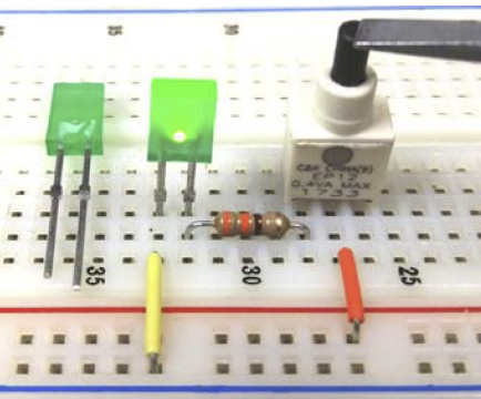
Figure 1.6: Simple resistor-LED circuit with a pushbutton switch to turn on and off the LED.
Build the circuit shown in Figure 1.6, which is just Figure 1.4 with the switch of Fig. 1-5 added. The resistor's value here is 330 ohms. A screwdriver is shown depressing the switch, thereby internally connecting the switch's center and left-hand leads. This allows current to flow up from the 5V (red) bus to the center lead and out the left-hand lead to the resistor. Current then flows through the resistor into the LED's anode and out of its cathode (thus turning it on) down to the ground (blue) bus. The resistor prevents excess current from flowing through the LED.
Question
- The LED's leads are not of equal length (as the one on the left illustrates). The longer one connects to the LED's anode and must be inserted next to the resistor. If you reverse the leads, the current can't flow; an LED is a diode and can only conduct in one direction. Press and release the pushbutton switch and record your observations.
Exp #1.4 * Transistor as a Switch
Part A
There are times when you want to control a circuit automatically rather than manually. Consider your air conditioner at home. You could turn it on and off manually, or you can use a thermostat that has a sensor to measure the temperature and a control system to turn the air conditioner on or off in order to maintain the desired temperature. In this case, you need to have a switch that can be controlled electronically. Transistors are electronic switches. Figure 1.7 shows the circuit diagram for an NPN transistor.
(Note: In this experiment, we want to have a basic understanding of what transistors are and how they work, but we will not be able to explore the physics behind semiconductor transistors. You will learn more about transistors in EE 2040 and EE 3700.)
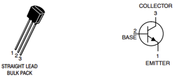
Figure 1.7: An NPN Transistor, an electronic (semiconductor) switch.
How is an NPN Transistor like a mechanical switch? The transistor is turned on when a small current flows into its base. This small current will induce a much larger current to flow from the collector to the emitter which can be used, for example, to turn on an LED like the one in Figure 1.8. Conversely, when the base current is cut off, no current flows from the collector to the emitter, and the LED is turned off.
Part B * (* = Lab Work)
Exp #1.4 Circuit Connection for On-Campus Lab
Figure 1.8 shows how to connect the transistor to our simple resistor-LED circuit to control turning the LED on and off.
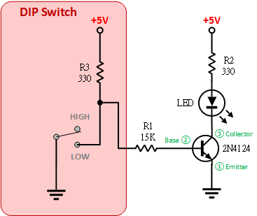
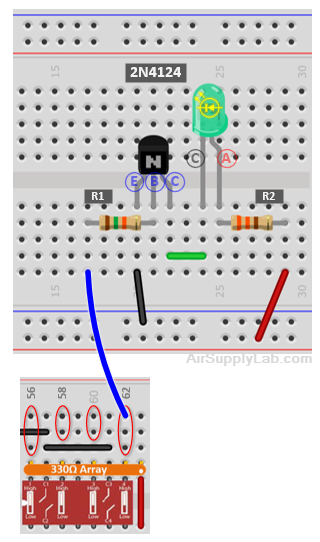
Figure 1.8: Resistor-LED Circuit Controlled by an NPN Transistor.
Build the circuit of Figure 1.8. Record observations in your journal as you open and close the switch.
- Connect the transistor's emitter pin directly to the ground.
- Connect the collector pin of the transistor with an LED and connect it to +5V through a 330-ohm resistor.
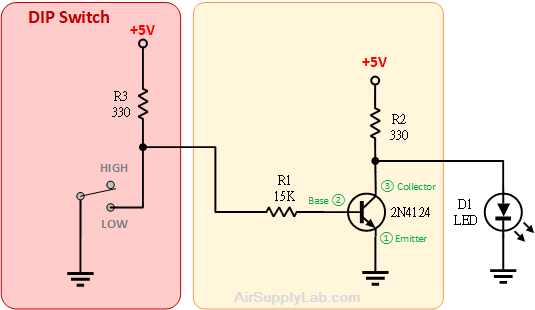
- Then, connect the base resistor (R1) to the output of one of the 12 toggle switches, and one of the DIP switch pins. (Pin 44, 46, 48, 50, 52, 54, 56, 58, 60, and 62)
As shown in Figure 1.8, when the switch is down, the output connects to the ground. When it is up, the switch is not connected (n/c) so the current can flow into R1 and the base from the 5V bus through an R3 (330Ω) "pullup" resistor. The voltage drop across this resistor will be very low, so we can say that the switch output is "pulled up" to just under 5V. The real purpose of the resistor is to prevent a short-circuit from 5V directly to the ground when the switch is down.
Question
- Describe your observation of the experiment in the report.
Exp #1.5 * Build a NOT gate Circuit
Transistors are the building blocks of digital logic circuits. Digital logic uses binary logic signals that are high (logic 1) and low (logic 0). Why binary? When a transistor is used as a switch and it has only two states: off or on, which can refer to the logical values: logic 0 (False) or logic 1 (True).
A simple logic function is the NOT function. If the input to the function is True (1) then the output is False (0) and vice-versa. We can describe the behavior of a logic circuit using a "truth table". The inputs to the logic function are shown on the left of the table and the corresponding outputs are shown on the right.
| Input | Output |
|---|---|
| False | True |
| True | False |
| Input | Output |
|---|---|
| 0 | 1 |
| 1 | 0 |
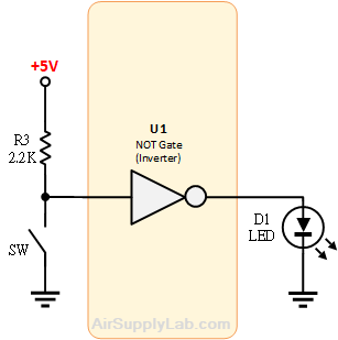
A NOT function (also known as an INVERTER) can be built using transistors. We refer to basic digital logic circuits as "gates". Other basic logic functions include AND, OR, XOR, NAND, NOR, and XNOR gates. You will learn more about these in Lab 03. Figure 1.10 shows the symbol of a NOT gate and the circuit to build it using an NPN transistor and Resistors.
Exp #1.5 Circuit Connection for On-Campus Lab
(a) The Circuit Built with an INVERTER Gate.
(b) Circuit for an INVERTER Function Built with a Discrete Transistor
Figure 1.10: INVERTER Circuits: With Gate and with Transistor
Based on your understanding of how the transistor works, you can see how the circuit in Figure 1.10 (b) will act as an INVERTER. It is behavior is as follows:
- When the switch is closed, input is grounded so there is no voltage across R1 and, therefore, no base current; instead all current flows down through R3 to the ground. As a result, the transistor does not conduct and current through R2 is diverted into the LED, turning it on. Thus, when the input goes low, the output goes high (LED on).
- When the switch is open, current flows through R3 and R1 into the transistor base. The transistor conducts, pulling the collector voltage almost to zero (the transistor saturates). This cuts off current into the LED. Thus when the input goes high (open switch), the output goes low (LED off).
Build the circuit of Figure 1.11. Record observations in your journal as you press and release the switch.
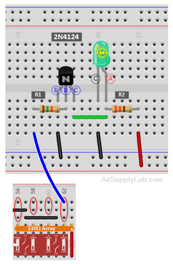
Figure 1.11: The Circuit of a NOT Function
(Note: Collector resistor R2 provides protection in two ways.
- When the switch is open, the transistor saturates and the collector voltage is essentially 0V. R2 limits the current flowing from the 5V supply ( ${I_C} = {5 \over {{R_2}}}$ ). But if R2 were 0, there would be excessive current flow into the collector which would likely blow the transistor.
- When the switch is closed, the transistor does not conduct and no current flows into the collector. R2 limits the current flowing into the LED which might otherwise also likely blow.
Now that you understand more about how electric circuits work, please refer to the test circuit description and schematic in KB07: Build the Test Circuit Component and Jumper Layout. Use your logic probe to verify that the test-circuit inputs all work properly; i.e. pushbutton switch outputs, toggle switch outputs (12), and 555 timer output. For the timer output, switch the large vertical (cylindrical) 470 μF capacitor into the timer circuit by moving the select switch toward the other capacitor. With the cylindrical one thus connected, the timer output frequency is a slow 1 Hz.
Clock output: Check the timer circuit's output with the logic probe. If the timer is working, the probe's LEDs should flash red and green at 1-second intervals--easy to detect. Now, move the capacitor and select switch the other way. This brings the 0.47 μF capacitor (much smaller value) into the circuit and the timer frequency jumps to 1,000 Hz. The probe LEDs again flash red and green but so rapidly that the eye can not see them flashing--they appear to be on all the time.
For the test circuit's LED bargraph chip, check it by connecting a wire from the push-button switch to each LED in sequence. Make sure each one turns on and off.
Question
- Describe your observation of this experiment in the report.