KB05: Implementing and Troubleshooting Designs
Wiring Techniques
One technique to help you avoid wiring errors is to make a photocopy of your design. Then, as you connect wire after wire, use an accent marker to color in each completed connection. Another thing you can do is to place a piece of tape or a small peel-off label indicating the unit number on each chip. Now, checking the connection U2-3 to U3-9 (or just 2-3 to 3-9) becomes quick and easy. Take your time making these connections. Most of the problems encountered in the lab are not due to bad chips (although many people tend to blame their trouble on the chips).
By far the most common causes of trouble are incorrect or missing connections. And one of the things that make it so difficult to spot a bad connection is the "spaghetti" or "ramen" approach to wiring: dozens of wires arching over the chips like a dense mass of cold, stiff noodles. This makes it hard to see where the wires go, and nearly impossible to remove a chip if one should turn out to be bad after all.
The alternative to spaghetti wiring is to cut all wires to the proper length, run them flat along the board with each bend at 90 degrees (you will have to leave room between the chips for the wires). Of course, this takes time to do and nobody wants to bother. But the savings in time and effort later when you are troubleshooting will make it all seem worthwhile. Your breadboard should come with a wire kit containing pre-cut wires with stripped and bent ends. Each of these spans an integral number of holes. Instead of bending a long wire around a corner, just insert two shorter lengths of wire at right angles to each other. Insertion and removal is done quickly and easily with a pair of tweezers or needle-nose pliers.
Debugging Combinational Circuits
A combinational circuit is one with no flip-flops or latches. You usually become aware of problems in combinational circuits when a check reveals that one or more outputs are at the wrong logic levels. The problem may be some or all of the following:
- the circuit contains one or more bad elements.
- you forgot to make certain connections.
- you made some incorrect connections.
The search for the source of trouble begins with finding an input combination that produces incorrect output. For this input combination, check your wiring diagram and determine what the correct values should be at the inputs and outputs of each gate involved in producing the output value. With a logic probe, begin working backward from the output, checking the value on each pin and using your wiring diagram "pinout" to guide you from pin to pin.
Example: you are checking a NAND gate whose output should be high. Instead, you find that it is low. Check the inputs. Usually, if a NAND output is low, all inputs should be high; but, if at least one input is low, the gate may be bad. Otherwise, if they are all high, the gate is probably ok but at least one of the circuits that produce the gate inputs is not. Check these circuits the same way.
Occasionally your logic probe fails to indicate either high or low. Possible explanations are:
- Bent Pin: if you get no indication when the probe touches a chip pin, the pin may be bent up under the chip and not in its hole (or the pin may be broken off).
- Input-Pin Connected to Only Inputs: check to see if a connecting wire which is supposed to go to an output pin actually goes to another input by mistake. If connections are made only to inputs, there will be no voltage to light up the probe.
- Output-Pin Connected to Another Output: if one output is high and the other low, the resulting voltage may be in-between (neither logic-1 nor logic-0), so a logic probe will indicate nothing. To check for this, disconnect all wires from the output of interest. If the probe now lights up, see if any of the wires going to another output by mistake.
Debugging Sequential Circuits
A sequential circuit (made up of flip-flops, like a counter) is designed to go through a particular sequence of states. Suppose at some point it makes an incorrect state transition. The wrong way to start debugging this circuit would be to begin an exhaustive check of all connections and voltage levels. There is a more efficient, logical approach. For the sake of example, consider a 4-bit synchronous sequential circuit with D-flip-flops W, X, Y, and Z. Each time the circuit is clocked, inputs, Dw, Dx, Dy, Dz are loaded into the flip-flops. Thus the next-state values of flip-flop outputs WXYZ are the same as the present-state values of their inputs.
Assume flip-flops W, X, Y, and Z are designed to follow the sequence ...0010 → 0100 → 1010... Now, suppose from state 0100, the circuit's next state goes to 1000, instead of 1010 as desired. In other words:

To locate the problem in a logical and systematic way, try the following approach:
- First, go back to your design. Verify that your state table is correct. Do the same for the maps and for the algebraic expressions derived from the maps. Checking your design on paper is usually much simpler than debugging the hardware.
- If the design seems ok, place your circuit in the state from which the incorrect transition is made. In the example we are using, this would be stated WXYZ = 0100. Notice that in going from 0100 to 1000, all flip-flops undergo the designed-for transition except Y, which fails to go high. Therefore, the obvious place to check is input Dy (while still in state 0100).
- When you check with the 'scope or logic probe, you expect to find Dy low since Y stays low after the next clock pulse. If instead, you find Dy to be high, there may be something wrong with the flip-flop. But, if it is low, go back and make sure you didn't design Dy to be low by mistake.
- Now, if your design is ok, the problem must lie with the circuit that produces Dy. If Dy comes from the output of a gate, go back to Section 3 (Debugging Combinational Circuits), above. Start by checking the wire that connects Dy to the gate. If the wire is properly connected, then check the gate and its inputs, etc.
- When working with sequential circuits, make sure that your asynchronous preset and clear inputs are connected to the supply voltage (5V) if they are not being used.
Troubleshooting a Circuit using Maps
This section is designed to be used in situations where counter outputs are used to test a circuit by applying all possible input combinations in a binary sequence. Assume the counter is triggered with a square pulse output, where the circuit output is monitored with an LED.
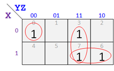
Suppose you build a circuit for the function F = X Y Z + Y Z + X Y. Since a 3-input AND is not available, two 2-input ANDs are required for the first term; i.e. (X • Y) • Z. The last two terms require two more ANDs, so together with the two OR gates (+, +), a total of 6 gates are needed.
The map for F, derived from the equation, is below.

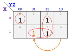
Now suppose that you build the circuit from the equation for F and drive it with outputs from the counter. You then record values for F as the counter goes through all 8 combinations in binary order. You insert F values into a map and get the result shown below. Since the two maps don't match, there's an error in the circuit.

Naturally, you could check connections among all the gates to see what's wrong. But it may also be possible to find the error instead of the differences between the two maps.
Note that the 1 in square 6 of the original map has moved to square 5, so that F = X Y Z + Y Z + X Z.
Conclusion: X Y in the original expression for F is replaced by X Z, implying that Z was mistakenly connected to the last AND gate (the last term in F) instead of Y.
(This method is fairly quick if only one incorrect connection is made to an AND gate, as in this case and the next.)
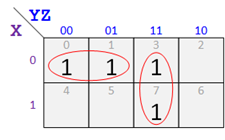
As another example, suppose your measured values for F lead to this map (the 1 in square 6 appears instead of in square 2). By grouping the 1's as shown below, this could be simplified as F = X Y + Y Z. But that would imply a design of form F = xx + xx (2 ANDs and 1 OR) which is not like the circuit you built where F = xxx + xx + xx.

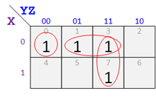
So rather than over-simplify, try instead to maintain the form of the original equation if possible. Grouping the 1's as in the below map, we get F = X Y Z + Y Z + X Z.

Here the mistake was connecting X to the last gate instead of X.
A final word: efficient debugging requires practice as well as theoretical knowledge. You already have the theory, and you'll be surprised at how your self-confidence grows with a bit of practice and a few small successes. So when your circuit doesn't work as planned, don't throw up your hands. Pick up your logic probe and find the bug.