Tiva Lab 09: Using UART to Communicate with Host PC
Objective
- Understand how to do a project with a UART on the Tiva board and then how to communicate through that connection.
Required Reading Material
- Lesson 10: GPIO Port Control Register (GPIOPCTL)
- Lesson 15: Universal Asynchronous Receiver Transmitter (UART)
- Windows software for serial communication: [Termite Website] Download Termite 3.4: [exe] [zip]
- Windows software for serial communication: PuTTY.exe: http://www.chiark.greenend.org.uk/~sgtatham/putty/latest.html
Background Information
The most basic method for communication with an embedded processor is asynchronous serial. UARTs are now commonly included in microcontrollers such as the TI Tiva LaunchPad we are working on. In this lab, you will be building serial communication between the TI Tiva microcontroller and the host PC. On the Tiva LauncdPad boards, one of the UARTs connected to the emulation hardware (In-Circuit Debugger Interface: ICDI), which then connects through the USB port to your PC. On the PC, the UART connection will appear as a virtual COM port in the Windows "Device Manager."
Universal Asynchronous Receiver-Transmitter (UART)
A Universal Asynchronous Receiver/Transmitter, abbreviated UART (pronounced ' you-art '), is an asynchronous serial communication protocol. The universal designation indicates that the data format and transmission speeds are configurable. UART is a very useful interface that can transmit signals without needing to synchronize with a clock signal. This method of transmission is extremely useful for reducing wires and I/O pins compared to parallel systems which transmit data faster but are far more complex. It provides a cost-effective simple and reliable communication between one controller to another controller or between a controller and host computer.
In the UART system, the parallel data is reformatted into a serial stream and then sent out through the transmitting wire. In the simplest connection form, a UART can be thought of as a two-wire communication system where one line is transmitting and the other is receiving. UART can be configured for Full Duplex, Half Duplex, RX-only, or TX-only versions.
UARTs are commonly used in conjunction with a communication standard such as RS-232 or RS-485. The voltage levels of RS-232 are -12V and +12V. Usually, all the digital systems work on TTL or CMOS voltage levels, which are not directly compatible with those of RS-232, a level transition buffer such as MAX232 must be used.
Data Packet Format
UART-transmitted data is organized into packets. Each packet contains [1 START bit ] + [ DATA frame (5 ~ 9 bits) ] + [ PARITY bit (optional) ] + [ STOP bit (1, 2) ], as shown in the following diagram.
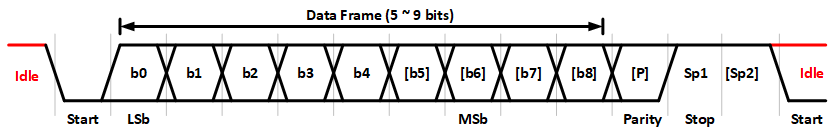
- START bit
In the Idle mode, the UART data line is held at a high voltage level (logic 1). To start data transmission, the transmitting UART pulls the transmission line to low for one clock cycle. When the receiving UART detects the data line from high to low voltage transition, it begins reading the bits in the data frame at the frequency of the baud rate. - DATA frame
The data frame contains the data being transferred. Options are 5, 6, 7, 8 (default), or 9. If the PARITY bit is not used, the length of the data frame could be up to 9 bits; if a parity bit is used, the maximum length of the data frame is up to 8 bits. - PARITY bit
The parity bit is for error checking when the receiving UART receives a packet. This can be set to None (default), Odd, Even, or Mark/Space. If the data frame is 9-bits, then the Parity type must be Mark/Space. The parity bit is optional and it is actually not that widely used. - STOP bits
To signal the end of the data packet, the sending UART drives the data transmission line from a low voltage to a high voltage. The STOP bit can be set to 1 (default) or 2 bits.
Baud Rate
The baud rate specifies how fast data is sent over a serial line. The units of the baud rate are bit-per-second (bps). The higher the baud rate goes, the faster data is sent and received, but the speed of data transfer is limited. Since there is no clock signal in the UART communication, the higher transmitting speed will easily lead to errors on the receiving end. Therefore, each of the two UARTs must be communicating using a known baud rate or bit frequency. The receiver and transmitter clock rates must be within 5% to avoid errors.
There are different sets of standard baud dates used depending on the application. Usually, the baud rates use 1200, 2400, 4800, 9600,19200, 38400, 57600 and 115200 bps. Both the local and remote UARTs must be configured for the same baud rate.
How does UART work?
UARTs transmit data asynchronously, which means there is no clock signal to synchronize the data bits from the transmitting UART to the receiving UART. Typically, asynchronous communication needs handshaking signals to ensure sender and receiver coordinate data transfers. In the UART, there are no extra handshaking signals between the transmitter and receiver. The transmitter generates a bitstream based on its clock signal, and then the receiver's goal is to use its internal clock signal to sample the incoming data. Therefore, the transmitter and receiver both need to have the same transfer speed and data packet format. Then, the receiver's UART resynchronizes the internal clocks on the falling edge of the start bit and then reads the center of each expected data bit based on the baud rate that is set.
UART Flow Control
UART Flow Control is a method for slow and fast devices to communicate with each other over UART without the risk of losing data.
Consider the case where two units are communicating over UART. A transmitter T is sending a long stream of bytes to a receiver R. R is a slower device than T, and at some point, R cannot keep up. It needs to either do some processing on the data or empty some buffers before it can keep receiving data.
R needs to tell T to stop transmitting for a while. This is where flow control comes in. Flow control provides extra signaling to inform the transmitter that it should stop (pause) or start (resume) the transmission.
Several forms of flow control exist. For example, hardware flow control uses extra wires, where the logic level on these wires defines whether the transmitter should keep sending data or stop. With software flow control, special characters are sent over the normal data lines to start or stop the transmission.
Hardware Flow Control: also called RTS/CTS Flow Control
When hardware flow control is enabled, two extra wires are needed in addition to the data lines. They are called RTS (Request to Send) and CTS (Clear to Send). The CTS signal is an input to the UART that is set by the other UART in the system when it is OK to send data on the bus. The RTS signal is an output of the UART informing the other UART on the bus that it is ready to receive data. The RTS line of one UART is connected to the CTS line of the other UART and vice versa. These lines are only valid before transmission is started. If the signal is set or cleared after a transfer is started the change will only affect the next transfer.
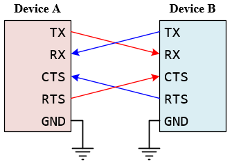
Figure 2: The Connection for Hardware Flow Control
Software Flow Control
Software flow control does not use extra wires. Only 3 wires are required (RX, TX, and GND). Transmission is started and stopped by sending special flow control characters. The flow control characters are sent over the normal TX and RX lines. The flow control characters are typically the ASCII codes XON and XOFF (0x11 and 0x13). If device A sends XOFF to device B it means that B should halt transmission to A until B receives an XON character from A.
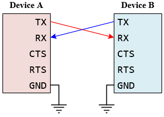
Figure 3: The Connection for Software Flow Control
UART Configurations
Both UART communicating devices must operate at the same baud rate and have the same configuration for successful communication:
- Baud Rate
- Standard Mode: 110 to 115,200 bps
- Fast Mode: 230,400 ~ 921,600 bps, up to 4 Mbps
- Modes: Full-duplex, half-duplex, TX only, RX only
- Data Bits: 5 ~ 9 bits
- Endianess: Some UART devices offer the option to send the data in either LSb or MSb. The UART is almost always LSb.
- Parity Types: None, Even, Odd, Mark/Space
- Stop Bits: 1 or 2
- Flow Control: None, Hardware (CTS/RTS), Software (Xon/Xoff)
The most common configuration for UART is often listed as "8N1", which is shorthand for eight data bits, no parity, and one-stop bit. This is the default configuration for the UART communication protocol. Therefore, in most applications, you only need to set the baud rate.
Required Components List
  |
Breadboard Power Module | × 1 |
| Power Adapter | × 1 | |
| DC Motor / Fan | × 1 | |
| Breadboard | × 1 |
Circuit / Schematic Diagram
Procedure
- Create a new folder under the EE3450 folder and name it Lab09_UART.
- Launch the Keil μVisio and create a new project. Save the project to the project folder you just created in the previous step and set the project name to Lab09_UART.
- Add the Common and ezTivaLIB folders to the include paths, that is under the "Options for Target" setting.
- Add ezTiva LIB (ez123GLIB.lib or ez1294LIB.lib) into your project, increase the stack and heap size under the "startup_TM4cXXX.s (Startup)" setting.
MyDefines.H
Add the following definitions to the MyDefines.h file:


Configurations
Pin Connection and Configuration
EK-TM4C123GXL LaunchPad
| Device | Port.Pin | Signal Type | PCTL | Direction | Drive Mode |
|---|---|---|---|---|---|
EK-TM4C1294XL LaunchPad
| Device | Port.Pin | Signal Type | PCTL | Direction | Drive Mode |
|---|---|---|---|---|---|
GPIO Port Control Register (GPIOPCTL)
Lesson 10: GPIO Port Control Register (GPIOPCTL)
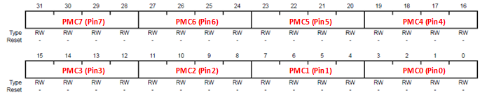
The GPIOPCTL register is used in conjunction with the GPIOAFSEL register and selects the specific peripheral signal for each GPIO pin when using the alternate function mode. Most bits in the GPIOAFSEL register are cleared on reset, therefore most GPIO pins are configured as GPIOs by default. When a bit is set in the GPIOAFSEL register, the corresponding GPIO signal is controlled by an associated peripheral. The GPIOPCTL register selects one out of a set of peripheral functions for each GPIO, providing additional flexibility in signal definition. Following tables are the information on the defined encodings for the bit fields in this register.
TM4C123G MCU
| I/O | Analog Function |
Digital Function (GPIOx->PCTL PMCn Field Encoding) | |||||||||||||||
| 0x0 | 0x1 | 0x2 | 0x3 | 0x4 | 0x5 | 0x6 | 0x7 | 0x8 | 0x9 | 0xA | 0xB | 0xC | 0xD | 0xE | 0xF | ||
| 0000 | 0001 | 0010 | 0011 | 0100 | 0101 | 0110 | 0111 | 1000 | 1001 | 1010 | 1011 | 1100 | 1101 | 1110 | 1111 | ||
| PA0 | — | GPIO | U0Rx | — | — | — | — | — | — | CAN1Rx | — | — | — | — | — | — | — |
| PA1 | — | GPIO | U0Tx | — | — | — | — | — | — | CAN1Tx | — | — | — | — | — | — | — |
| PA2 | — | GPIO | — | SSI0CLK | — | — | — | — | — | — | — | — | — | — | — | — | — |
| PA3 | — | GPIO | — | SSI0Fss | — | — | — | — | — | — | — | — | — | — | — | — | — |
| PA4 | — | GPIO | — | SSI0Rx | — | — | — | — | — | — | — | — | — | — | — | — | — |
| PA5 | — | GPIO | — | SSI0Tx | — | — | — | — | — | — | — | — | — | — | — | — | — |
| PA6 | — | GPIO | — | — | I2C1SCL | — | M1PWM2 | — | — | — | — | — | — | — | — | — | — |
| PA7 | — | GPIO | — | — | I2C1SDA | — | M1PWM3 | — | — | — | — | — | — | — | — | — | — |
| PB0 | USB0ID | GPIO | U1Rx | — | — | — | — | — | T2CCP0 | — | — | — | — | — | — | — | — |
| PB1 | USB0VBUS | GPIO | U1Tx | — | — | — | — | — | T2CCP1 | — | — | — | — | — | — | — | — |
| PB2 | — | GPIO | — | — | I2C0SCL | — | — | — | T3CCP0 | — | — | — | — | — | — | — | — |
| PB3 | — | GPIO | — | — | I2C0SDA | — | — | — | T3CCP1 | — | — | — | — | — | — | — | — |
| PB4 | AIN10 | GPIO | — | SSI2Clk | — | M0PWM2 | — | — | T1CCP0 | CAN0Rx | — | — | — | — | — | — | — |
| PB5 | AIN11 | GPIO | — | SSI2Fss | — | M0PWM3 | — | — | T1CCP1 | CAN0Tx | — | — | — | — | — | — | — |
| PB6 | — | GPIO | — | SSI2Rx | — | M0PWM0 | — | — | T0CCP0 | — | — | — | — | — | — | — | — |
| PB7 | — | GPIO | — | SSI2Tx | — | M0PWM1 | — | — | T0CCP1 | — | — | — | — | — | — | — | — |
| PC0 | — | GPIO | TCK SWCLK |
— | — | — | — | — | T4CCP0 | — | — | — | — | — | — | — | — |
| PC1 | — | GPIO | TMS SWDIO |
— | — | — | — | — | T4CCP1 | — | — | — | — | — | — | — | — |
| PC2 | — | GPIO | TDI | — | — | — | — | — | T5CCP0 | — | — | — | — | — | — | — | — |
| PC3 | — | GPIO | TDO SWO |
— | — | — | — | — | T5CCP1 | — | — | — | — | — | — | — | — |
| PC4 | C1- | GPIO | U4Rx | U1Rx | — | M0PWM6 | — | IDX1 | WT0CCP0 | U1RTS | — | — | — | — | — | — | — |
| PC5 | C1+ | GPIO | U4Tx | U1Tx | — | M0PWM7 | — | PhA1 | WT0CCP1 | U1CTS | — | — | — | — | — | — | — |
| PC6 | C0+ | GPIO | U3Rx | — | — | — | — | PhB1 | WT1CCP0 | USB0EPEN | — | — | — | — | — | — | — |
| PC7 | C0- | GPIO | U3Tx | — | — | — | — | — | WT1CCP1 | USB0PFLT | — | — | — | — | — | — | — |
| PD0 | AIN7 | GPIO | SSI3Clk | SSI1Clk | I2C3SCL | M0PWM6 | M1PWM0 | — | WT2CCP0 | — | — | — | — | — | — | — | — |
| PD1 | AIN6 | GPIO | SSI3Fss | SSI1Fss | I2C3SDA | M0PWM7 | M1PWM1 | — | WT2CCP1 | — | — | — | — | — | — | — | — |
| PD2 | AIN5 | GPIO | SSI3Rx | SSI1Rx | — | M0FAILT0 | — | — | WT3CCP0 | USB0EPEN | — | — | — | — | — | — | — |
| PD3 | AIN4 | GPIO | SSI3Tx | SSI1Tx | — | — | — | IDX0 | WT3CCP1 | USB0PFLT | — | — | — | — | — | — | — |
| PD4 | USB0DM | GPIO | U6Rx | — | — | — | — | — | WT4CCP0 | — | — | — | — | — | — | — | — |
| PD5 | USB0DP | GPIO | U6Tx | — | — | — | — | — | WT4CCP1 | — | — | — | — | — | — | — | — |
| PD6 | — | GPIO | U2Rx | — | — | M0FAULT0 | — | PhA0 | WT5CCP0 | — | — | — | — | — | — | — | — |
| PD7 | — | GPIO | U2Tx | — | — | — | — | PhB0 | WT5CCP1 | NMI | — | — | — | — | — | — | — |
| PE0 | AIN3 | GPIO | U7Rx | — | — | — | — | — | — | — | — | — | — | — | — | — | — |
| PE1 | AIN2 | GPIO | U7Tx | — | — | — | — | — | — | — | — | — | — | — | — | — | — |
| PE2 | AIN1 | GPIO | — | — | — | — | — | — | — | — | — | — | — | — | — | — | — |
| PE3 | AIN0 | GPIO | — | — | — | — | — | — | — | — | — | — | — | — | — | — | — |
| PE4 | AIN9 | GPIO | U5Rx | — | I2C2SCL | M0PWM4 | M1PWM2 | — | — | CAN0Rx | — | — | — | — | — | — | — |
| PE5 | AIN8 | GPIO | U5Tx | — | I2C3SDA | M0PWM5 | M1PWM3 | — | — | CAN0TX | — | — | — | — | — | — | — |
| PF0 | — | GPIO | U1RTS | SSI1Rx | CAN0Rx | — | M1PWM4 | PhA0 | T0CCP0 | NMI | C0o | — | — | — | — | — | — |
| PF1 | — | GPIO | U1CTS | SSI1Tx | — | — | M1PWM5 | PhB0 | T0CCP1 | — | C1o | — | — | — | — | TRD1 | — |
| PF2 | — | GPIO | — | SSI1Clk | — | M0FAULT0 | M1PWM6 | — | T1CCP0 | — | — | — | — | — | — | TRD0 | — |
| PF3 | — | GPIO | — | SSI1Fss | CAN0Tx | — | M1PWM7 | — | T1CCP1 | — | — | — | — | — | — | TRCLK | — |
| PF4 | — | GPIO | — | — | — | — | M1FAULT0 | IDX0 | T2CCP0 | USB0EPEN | — | — | — | — | — | — | — |
| I/O | Analog Function |
0000 | 0001 | 0010 | 0011 | 0100 | 0101 | 0110 | 0111 | 1000 | 1001 | 1010 | 1011 | 1100 | 1101 | 1110 | 1111 |
| 0x0 | 0x1 | 0x2 | 0x3 | 0x4 | 0x5 | 0x6 | 0x7 | 0x8 | 0x9 | 0xA | 0xB | 0xC | 0xD | 0xE | 0xF | ||
| Digital Function (GPIOx->PCTL PMCn Field Encoding) | |||||||||||||||||
PD7 and PF0 are configured as GPIO by default but is locked and can only be reprogrammed by unlocking the pin in the GPIOLOCK register and uncommitting it by setting the GPIOCR register.
TM4C1294 MCU
| I/O | Analog Function |
Digital Function (GPIOx->PCTL PMCn Field Encoding) | |||||||||||||||
| 0x0 | 0x1 | 0x2 | 0x3 | 0x4 | 0x5 | 0x6 | 0x7 | 0x8 | 0x9 | 0xA | 0xB | 0xC | 0xD | 0xE | 0xF | ||
| 0000 | 0001 | 0010 | 0011 | 0100 | 0101 | 0110 | 0111 | 1000 | 1001 | 1010 | 1011 | 1100 | 1101 | 1110 | 1111 | ||
| PA0 | — | GPIO | U0Rx | I2C9SCL | T0CCP0 | — | — | — | CAN0Rx | — | — | — | — | — | — | — | — |
| PA1 | — | GPIO | U0Tx | I2C9SDA | T0CCP1 | — | — | — | CAN0Tx | — | — | — | — | — | — | — | — |
| PA2 | — | GPIO | U4Rx | I2C8SCL | T1CCP0 | — | — | — | — | — | — | — | — | — | — | — | SSI0CLK |
| PA3 | — | GPIO | U4Tx | I2C8SDA | T1CCP1 | — | — | — | — | — | — | — | — | — | — | — | SSI0Fss |
| PA4 | — | GPIO | U3Rx | I2C7SCL | T2CCP0 | — | — | — | — | — | — | — | — | — | — | — | SSI0XDAT0 |
| PA5 | — | GPIO | U3Tx | I2C7SDA | T2CCP1 | — | — | — | — | — | — | — | — | — | — | — | SSI0XDAT1 |
| PA6 | — | GPIO | U2Rx | I2C6SCL | T3CCP0 | — | USB0EPEN | — | — | — | — | — | — | — | SSI0XDAT2 | — | EPI0S8 |
| PA7 | — | GPIO | U2Tx | I2C6SDA | T3CCP1 | — | USB0PFLT | — | — | — | — | — | USB0EPEN | — | SSI0XDA3 | — | EPI0S9 |
| PB0 | USB0ID | GPIO | U1Rx | I2C5SCL | T4CCP0 | — | — | — | CAN1Rx | — | — | — | — | — | — | — | — |
| PB1 | USB0VBUS | GPIO | U1Tx | I2C5SDA | T4CCP1 | — | — | — | CAN1Tx | — | — | — | — | — | — | — | — |
| PB2 | — | GPIO | — | I2C0SCL | T5CCP0 | — | — | — | — | — | — | — | — | — | — | USB0STP | EPI0S27 |
| PB3 | — | GPIO | — | I2C0SDA | T5CCP1 | — | — | — | — | — | — | — | — | — | — | USB0CLK | EPI0S28 |
| PB4 | AIN10 | GPIO | U0CTS | I2C5SCL | — | — | — | — | — | — | — | — | — | — | — | — | SSI1Fss |
| PB5 | AIN11 | GPIO | U0RTS | I2C5SDA | — | — | — | — | — | — | — | — | — | — | — | — | SSI1Clk |
| PC0 | — | GPIO | TCK SWCLK |
— | — | — | — | — | — | — | — | — | — | — | — | — | — |
| PC1 | — | GPIO | TMS SWDIO |
— | — | — | — | — | — | — | — | — | — | — | — | — | — |
| PC2 | — | GPIO | TDI | — | — | — | — | — | — | — | — | — | — | — | — | — | — |
| PC3 | — | GPIO | TDO SWO |
— | — | — | — | — | — | — | — | — | — | — | — | — | — |
| PC4 | C1- | GPIO | U7Rx | — | — | — | — | — | — | — | — | — | — | — | — | — | EPI0S7 |
| PC5 | C1+ | GPIO | U7Tx | — | — | — | — | — | RTCCLK | — | — | — | — | — | — | — | EPI0S6 |
| PC6 | C0+ | GPIO | U5Rx | — | — | — | — | — | — | — | — | — | — | — | — | — | EPI0S5 |
| PC7 | C0- | GPIO | U5Tx | — | — | — | — | — | — | — | — | — | — | — | — | — | EPI0S4 |
| PD0 | AIN15 | GPIO | — | I2C7SCL | T0CCP0 | — | C0o | — | — | — | — | — | — | — | — | — | SSI2XDAT1 |
| PD1 | AIN14 | GPIO | — | I2C7SDA | T0CCP1 | — | C1o | — | — | — | — | — | — | — | — | — | SSI2XDAT0 |
| PD2 | AIN13 | GPIO | — | I2C8SCL | T1CCP0 | — | C2o | — | — | — | — | — | — | — | — | — | SSI2Fass |
| PD3 | AIN12 | GPIO | — | I2C8SDA | T1CCP1 | — | — | — | — | — | — | — | — | — | — | — | SSI2Clk |
| PD4 | AIN7 | GPIO | U2Rx | — | T3CCP0 | — | — | — | — | — | — | — | — | — | — | — | SSI1XDAT2 |
| PD5 | AIN6 | GPIO | U2Tx | — | T3CCP1 | — | — | — | — | — | — | — | — | — | — | — | SSI1XDAT3 |
| PD6 | AIN5 | GPIO | U2RTS | — | T4CCP0 | — | USB0EPEN | — | — | — | — | — | — | — | — | — | SSI2XDAT3 |
| PD7 | AIN4 | GPIO | U2CTS | — | T4CCP1 | — | USB0OFLT | — | — | NMI | — | — | — | — | — | — | SSI2XDAT2 |
| PE0 | AIN3 | GPIO | U1RTS | — | — | — | — | — | — | — | — | — | — | — | — | — | — |
| PE1 | AIN2 | GPIO | U1DSR | — | — | — | — | — | — | — | — | — | — | — | — | — | — |
| PE2 | AIN1 | GPIO | U1DCD | — | — | — | — | — | — | — | — | — | — | — | — | — | — |
| PE3 | AIN0 | GPIO | U1DTR | — | — | — | — | — | — | — | — | — | — | — | — | — | — |
| PE4 | AIN9 | GPIO | U1RI | — | — | — | — | — | — | — | — | — | — | — | — | — | SSI1XDAT0 |
| PE5 | AIN8 | GPIO | — | — | — | — | — | — | — | — | — | — | — | — | — | — | SSIXDAT1 |
| PF0 | — | GPIO | — | — | — | — | EN0LED0 | M0PWM0 | — | — | — | — | — | — | — | SSI3XDAT1 | TRD2 |
| PF1 | — | GPIO | — | — | — | — | EN0LED2 | M0PWM1 | — | — | — | — | — | — | — | SSI3XDAT0 | TRD1 |
| PF2 | — | GPIO | — | — | — | — | — | M0PWM2 | — | — | — | — | — | — | — | SSI3Fss | TRD0 |
| PF3 | — | GPIO | — | — | — | — | — | M0PWM3 | — | — | — | — | — | — | — | SSI3Clk | TRCLK |
| PF4 | — | GPIO | — | — | — | — | EN0LED1 | M0FAULT0 | — | — | — | — | — | — | — | SSI3XDA2 | TRD3 |
| IO | Analog Function | Digital Function (GPIOx->PCTL PMCn Field Encoding) | |||||||||||||||
| 0x0 | 0x1 | 0x2 | 0x3 | 0x4 | 0x5 | 0x6 | 0x7 | 0x8 | 0x9 | 0xA | 0xB | 0xC | 0xD | 0xE | 0xF | ||
| 0000 | 0001 | 0010 | 0011 | 0100 | 0101 | 0110 | 0111 | 1000 | 1001 | 1010 | 1011 | 1100 | 1101 | 1110 | 1111 | ||
| PG0 | — | GPIO | — | I2C1SLC | — | — | EN0PPS | M0PWM4 | — | — | — | — | — | — | — | — | EPI0S11 |
| PG1 | — | GPIO | — | I2C1SDA | — | — | — | M0PWM5 | — | — | — | — | — | — | — | — | EPI0S10 |
| PH0 | — | GPIO | U0RTS | — | — | — | — | — | — | — | — | — | — | — | — | — | EPI0S0 |
| PH1 | — | GPIO | U0CTS | — | — | — | — | — | — | — | — | — | — | — | — | — | EPI0S1 |
| PH2 | — | GPIO | U0DCD | — | — | — | — | — | — | — | — | — | — | — | — | — | EPI0S2 |
| PH3 | — | GPIO | U0DSR | — | — | — | — | — | — | — | — | — | — | — | — | — | EPI0S3 |
| PJ0 | — | GPIO | U3Rx | — | — | — | EN0PPS | — | — | — | — | — | — | — | — | — | — |
| PJ1 | — | GPIO | U3Tx | — | — | — | — | — | — | — | — | — | — | — | — | — | — |
| PK0 | AIN16 | GPIO | U4Rx | — | — | — | — | — | — | — | — | — | — | — | — | — | EPI0S0 |
| PK1 | AIN17 | GPIO | U4Tx | — | — | — | — | — | — | — | — | — | — | — | — | — | EPI0S1 |
| PK2 | AIN18 | GPIO | U4RTS | — | — | — | — | — | — | — | — | — | — | — | — | — | EPI0S2 |
| PK3 | AIN19 | GPIO | U4CTS | — | — | — | — | — | — | — | — | — | — | — | — | — | EPI0S3 |
| PK4 | — | GPIO | — | I2C3SCL | — | — | EN0LED0 | M0PWM6 | — | — | — | — | — | — | — | — | EPI0S32 |
| PK5 | — | GPIO | — | I2C3SDA | — | — | EN0LED2 | M0PWM7 | — | — | — | — | — | — | — | — | EPI0S31 |
| PK6 | — | GPIO | — | I2C4SCL | — | — | EN0LED1 | M0FAULT1 | — | — | — | — | — | — | — | — | EPI0S25 |
| PK7 | — | GPIO | U0RI | I2C4SDA | — | — | RTCCLK | M0FAULT2 | — | — | — | — | — | — | — | — | EPI0S24 |
| PL0 | — | GPIO | — | I2C2SDA | — | — | — | M0FAULT3 | — | — | — | — | — | — | — | USB0D0 | EPI0S16 |
| PL1 | — | GPIO | — | I2C2SCL | — | — | — | PhA0 | — | — | — | — | — | — | — | USB0D1 | EPI0S17 |
| PL2 | — | GPIO | — | — | — | — | C0o | PhB0 | — | — | — | — | — | — | — | USB0D2 | EPI0S18 |
| PL3 | — | GPIO | — | — | — | — | C1o | IDX0 | — | — | — | — | — | — | — | USB0D3 | EPI0S19 |
| PL4 | — | GPIO | — | — | T0CCP0 | — | — | — | — | — | — | — | — | — | — | USB0D4 | EPI0S26 |
| PL5 | — | GPIO | — | — | T0CCP1 | — | — | — | — | — | — | — | — | — | — | USB0D5 | EPI0S33 |
| PL6 | USB0DP | GPIO | — | — | T1CCP0 | — | — | — | — | — | — | — | — | — | — | — | — |
| PL7 | USB0DM | GPIO | — | — | T1CCP1 | — | — | — | — | — | — | — | — | — | — | — | — |
| PM0 | — | GPIO | — | — | T2CCP0 | — | — | — | — | — | — | — | — | — | — | — | EPI0S15 |
| PM1 | — | GPIO | — | — | T2CCP1 | — | — | — | — | — | — | — | — | — | — | — | EPI0S14 |
| PM2 | — | GPIO | — | — | T3CCP0 | — | — | — | — | — | — | — | — | — | — | — | EPI0S13 |
| PM3 | — | GPIO | — | — | T3CCP1 | — | — | — | — | — | — | — | — | — | — | — | EPI0S12 |
| PM4 | TMPR3 | GPIO | U0CTS | — | T4CCP0 | — | — | — | — | — | — | — | — | — | — | — | — |
| PM5 | TMPR2 | GPIO | U0DCD | — | T4CCP1 | — | — | — | — | — | — | — | — | — | — | — | — |
| PM6 | TMPR1 | GPIO | U0DSR | — | T5CCP0 | — | — | — | — | — | — | — | — | — | — | — | — |
| PM7 | TMPR0 | GPIO | U0RI | — | T5CCP1 | — | — | — | — | — | — | — | — | — | — | — | — |
| PN0 | — | GPIO | U1RTS | — | — | — | — | — | — | — | — | — | — | — | — | — | — |
| PN1 | — | GPIO | U1CTS | — | — | — | — | — | — | — | — | — | — | — | — | — | — |
| PN2 | — | GPIO | U1DCD | U2RTS | — | — | — | — | — | — | — | — | — | — | — | — | EPI0S29 |
| PN3 | — | GPIO | U1DSR | U2CTS | — | — | — | — | — | — | — | — | — | — | — | — | EPI0S30 |
| PN4 | — | GPIO | U1DTR | U3RTS | I2C2SDA | — | — | — | — | — | — | — | — | — | — | — | EPI0S34 |
| PN5 | — | GPIO | U1RI | U3CTS | I2C2SCL | — | — | — | — | — | — | — | — | — | — | — | EPI0S35 |
| PP0 | C2+ | GPIO | U6Rx | — | — | — | — | — | — | — | — | — | — | — | — | — | SSI3XDAT2 |
| PP1 | C2- | GPIO | U6Tx | — | — | — | — | — | — | — | — | — | — | — | — | — | SSI3XDAT3 |
| PP2 | — | GPIO | U0DTR | — | — | — | — | — | — | — | — | — | — | — | — | USB0NXT | EPI0S29 |
| PP3 | — | GPIO | U1CTS | U0DCD | — | — | — | — | RTCCLK | — | — | — | — | — | — | USB0DIR | EPI0S30 |
| PP4 | — | GPIO | U3RTS | U0DSR | — | — | — | — | — | — | — | — | — | — | — | USB0D7 | — |
| PP5 | — | GPIO | U3CTS | I2C2SCL | — | — | — | — | — | — | — | — | — | — | — | USB0D6 | — |
| PQ0 | — | GPIO | — | — | — | — | — | — | — | — | — | — | — | — | — | SSI3Clk | EPI0S20 |
| PQ1 | — | GPIO | — | — | — | — | — | — | — | — | — | — | — | — | — | SSI3Fss | EPI0S21 |
| PQ2 | — | GPIO | — | — | — | — | — | — | — | — | — | — | — | — | — | SSI3XDAT0 | EPI0S22 |
| PQ3 | — | GPIO | — | — | — | — | — | — | — | — | — | — | — | — | — | SSI3XDAT1 | EPI0S23 |
| PQ4 | — | GPIO | U1Rx | — | — | — | — | — | DIVSCLK | — | — | — | — | — | — | — | — |
| I/O | Analog Function |
0000 | 0001 | 0010 | 0011 | 0100 | 0101 | 0110 | 0111 | 1000 | 1001 | 1010 | 1011 | 1100 | 1101 | 1110 | 1111 |
| 0x0 | 0x1 | 0x2 | 0x3 | 0x4 | 0x5 | 0x6 | 0x7 | 0x8 | 0x9 | 0xA | 0xB | 0xC | 0xD | 0xE | 0xF | ||
| Digital Function (GPIOx->PCTL PMCn Field Encoding) | |||||||||||||||||
PD7 and PE7 are configured as GPIO by default but is locked and can only be reprogrammed by unlocking the pin in the GPIOLOCK register and uncommitting it by setting the GPIOCR register.
UART Connection and Configuration
GPIO Initialization and Configuration
Example Source Code
EK-TM4C123GXL LaunchPad
Keil C Sample Code
#include <stdio.h>
#include <stdlib.h>
#include <stdbool.h>
#include <stdint.h>

#include "MyDefines.h"
#include "TM4C123GH6PM.h"
#include "ez123G.h"

void Setup_UART(void);
void Setup_GPIO(void);
void UART0_PrintString(char *s);

int main(void)
{
    char ch;
    char chNewLine = 10;
    char chReturn  = 13;
    int  i;

    Setup_123G_25MHz();  // Change the System Clock to 25Mhz
    Setup_UART();
    Setup_GPIO();

    while (1){
        ch = 'A';
        for (i = 0; i < 26; i++){
            while ((UART?->FR & ____ ) == ____) {};
            UART?->DR = ch;
            ezDelay(10);      // Hardware Delay
            ch ++;
        }
        while ((UART?->FR & ____) == ____) {};
        UART?->DR = chNewLine;
        while ((UART?->FR & ____) == ____) {};
        UART?->DR = chReturn;
        ezDelay(10);         // Hardware Delay
    }
}
//-------------------------------------------------------------------
void Setup_UART(void)  // UART Setting=115200,8N1
{
#define UARTIBRD 00     // You need to calculate IBRD value
#define UARTFBRD 00     // You need to calculate FBRD value

    // 1. Enable clock to UART Module (SYSCTL_RCGCUART)
    SYSCTL->RCGCUART |= (__);
    // allow time for clock to stabilize
    while ((SYSCTL->PRUART & (__) ) != (__)){};
    // 2. Disable UART by clearing UARTEN in UARTCTL register
    UART?->CTL &= ~(__);
    // 3. Write BRD to UARTIBRD and UARTFBRD register
    UART?->IBRD = UARTIBRD;
    UART?->FBRD = UARTFBRD;
    // 4. Write UART Line Control, High Byte (UARTLCRH register)
    //    8bit, No parity, 1-stop bit, Enable FIFO
    UART?->LCRH = ____;
    // 5. Configure the UART clock source (UARTCC register)
    UART?->CC = ____;   // Clock Source from System Clock
    // 6. Enable UART by clearing UARTEN in UARTCTL register
    UART?->CTL = ____; // Enable UART, TXE, RXE, UART High-Speed
}
//-------------------------------------------------------------------
void Setup_GPIO(void)
{
    // Enable PA0, PA1 for UART
    // GPIO Initialization and Configuration
    // 1. Enable Clock to the GPIO Modules (SYSCTL->RCGCGPIO |= (_PORTs);)
    SYSCTL->RCGCGPIO |= (__);
    // allow time for clock to stabilize (SYSCTL->PRGPIO)
    while ((SYSCTL->PRGPIO & (__)) != (__) ){};
    // 2. Unlock GPIO only PD7, PF0 on TM4C123G; PD7, PE7 on TM4C1294 (GPIOx->LOCK = 0x4C4F434B; and GPIOx->CR = _PINs;)
    // 3. Set Analog Mode Select bits for each Port (GPIOx->AMSEL = _PINs; 0=digital, 1=analog)
    // 4. Set Port Control Register for each Port (GPIOx->PCTL = PMCn << _PTCL_PINn, check the PCTL table)

    // 5. Set Alternate Function Select bits for each Port (GPIOx->AFSEL = _PINs; 0=regular I/O, 1=PCTL peripheral)

    // 6. Set Output pins for each Port (Direction of the Pins: GPIOx->DIR = _PINs; 0=input, 1=output)
    // 7. Set PUR bits for internal pull-up, PDR for pull-down reg, ODR for open drain (0: disable, 1=enable)
    // 8. Set Digital ENable register on all GPIO pins (GPIOx->DEN = _PINs; 0=disable, 1=enable)

}
//-------------------------------------------------------------------
void UART0_PrintString(char *s)
{

}
EK-TM4C1294XL LaunchPad
Keil C Sample Code
#include <stdio.h>
#include <stdlib.h>
#include <stdbool.h>
#include <stdint.h>

#include "MyDefines.h"
#include "TM4C1294NCPDT.h"
#include "ez1294.h"

void Setup_UART(void);
void Setup_GPIO(void);
void UART0_PrintString(char *s);

int main(void)
{
    char ch;
    char chNewLine = 10;
    char chReturn  = 13;
    int  i;

    Setup_1294_48MHz();  // Change the System Clock to 48Mhz
    Setup_UART();
    Setup_GPIO();

    while (1){
        ch = 'A';
        for (i = 0; i < 26; i++){
            while ((UART?->FR & ____ ) == ____) {};
            UART?->DR = ch;
            ezDelay(10);    // Hardware Delay
            ch ++;
        }
        while ((UART?->FR & ____) == ____) {};
        UART?->DR = chNewLine;
        while ((UART?->FR & ____) == ____) {};
        UART?->DR = chReturn;
        ezDelay(10);        // Hardware Delay
    }
}
//-------------------------------------------------------------------
void Setup_UART(void) // UART Setting=115200,8N1
{
#define UARTIBRD 00     // You need to calculate IBRD value
#define UARTFBRD 00     // You need to calculate FBRD value

    // 1. Enable clock to UART Module (SYSCTL_RCGCUART)
    SYSCTL->RCGCUART |= (__);
    // allow time for clock to stabilize
    while ((SYSCTL->PRUART & (__) ) != (__)){};
    // 2. Disable UART by clearing UARTEN in UARTCTL register
    UART?->CTL &= ~(__);
    // 3. Write BRD to UARTIBRD and UARTFBRD register
    UART?->IBRD = UARTIBRD;
    UART?->FBRD = UARTFBRD;
    // 4. Write UART Line Control, High Byte (UARTLCRH register)
    //    8bit, No parity, 1-stop bit, Enable FIFO
    UART?->LCRH = ____;
    // 5. Configure the UART clock source (UARTCC register)
    UART?->CC = ____;   // Clock Source from System Clock
    // 6. Enable UART by clearing UARTEN in UARTCTL register
    UART?->CTL = ____; // Enable UART0, TXE, RXE, UART High-Speed
}
//-------------------------------------------------------------------
void Setup_GPIO(void)
{
    // Enable PA0, PA1 for UART
    // GPIO Initialization and Configuration
    // 1. Enable Clock to the GPIO Modules (SYSCTL->RCGCGPIO |= (_PORTs);)
    SYSCTL->RCGCGPIO |= (__);
    // allow time for clock to stabilize (SYSCTL->PRGPIO)
    while ((SYSCTL->PRGPIO & (__)) != (__) ){};
    // 2. Unlock GPIO only PD7, PF0 on TM4C123G; PD7, PE7 on TM4C1294 (GPIOx->LOCK = 0x4C4F434B; and GPIOx->CR = _PINs;)
    // 3. Set Analog Mode Select bits for each Port (GPIOx->AMSEL = _PINs; 0=digital, 1=analog)
    // 4. Set Port Control Register for each Port (GPIOx->PCTL = PMCn << _PTCL_PINn, check the PCTL table)

    // 5. Set Alternate Function Select bits for each Port (GPIOx->AFSEL = _PINs; 0=regular I/O, 1=PCTL peripheral)

    // 6. Set Output pins for each Port (Direction of the Pins: GPIOx->DIR = _PINs; 0=input, 1=output)
    // 7. Set PUR bits for internal pull-up, PDR for pull-down reg, ODR for open drain (0: disable, 1=enable)
    // 8. Set Digital ENable register on all GPIO pins (GPIOx->DEN = _PINs; 0=disable, 1=enable)

}
//-------------------------------------------------------------------
void UART0_PrintString(char *s)
{

}
- Connect your Tiva board to a USB port on the computer.
- Build your code. You have to fix all the syntax errors, and then program the code to the Tiva board.
- Launch the Device Manager to find the COM port number.

- Launch the Termite (or PuTTY) program. Change the COM port number and settings, which must be the same as the UART Configuration in the Tiva code, and then click Open to connect the PC to the Tiva board.
- If your UART and GPIO are configured correctly, you will see characters from 'A' to 'Z' on the PC screen.
Lab Experiments
Exp #9.1: Send a string message over UART
In the example source code, it one character is sent to the UART every time. Now, you must modify the code to implement a function that can send a message (string) to UART.
- Create a function void UART0_PrintString(const char* str) to send a message to the UART Tx.
- Modify the example source code to continuously send the string "Hello, My name is XXXX \n\r" (the xxx is your first name) to the PC using the UART0_PrintString() function.
char str[20]; char *myName = "YourName"; .... while (1){ sprintf(str, "Hello, My name is %s \r\n", myName); UART0_PrintString( str); ezDelayUs(500); // Hardware Delay: 500 us } - At the end of the source code, add the UART0_PrintString() function:
void UART0_PrintString(char *s)
{


}
Questions
- What is the meaning of the 2400,8O2 configuration for a UART?
- Configure the UART clock source to the system clock, then set the system clock to 25 MHz and the ClkDiv to 16. What are the values for UARTIBRD and UARTFBRD registers if the baud rate is 9600 bps?
Exp #9.2: Send commands from PC to TIVA board through UART
In this experiment, you have to use the Termite program to send the command to your Tiva board.
In the Termite program, click the Settings button to configure the Termite as shown in the following picture.
- Change the Port configuration based on the serial port on Windows and the UART settings on the Tiva board.
- If the stop character is "\r\n", then you have to change the Transmitted text to Append CR-LF. Otherwise, set the Transmitted text to Append nothing.
- Unchecked the Local echo

The command format should follow:
[Start Character] [Command] [Stop Characters]
In this lab, we used the '+' character as the start character and the '\r\n' as the stop character.
In the Termite Settings tab, you must set the Transmitted text to Append CR-LF. Therefore, when you press the Enter key, the Termite software will automatically add '\r\n' at the end of the string. If you want to send a command to turn on the LED1, you just need to type +LCD1ON and press Enter key (do not type \r\n in the command line) to send the command to your Tiva board.
Part A
Now, add two LEDs into your design and the following predefined command strings to control those LEDs:
| Command String | Description |
|---|---|
| LED1ON | Turn on LED1 |
| LED1OFF | Turn off LED1 |
| LED2ON | Turn on LED2 |
| LED2OFF | Turn off LED2 |
Once you send the command string from the Termite software, your Tiva board needs to execute the command and send a response message back to the PC so the controller (you) can know that the Tiva board got your command.
You should define your own response message for each command. For example, you can define the response message for the LED1ON command as 'The LED1 is on now.'.
Type the following commands on the Termite program:
- +LED1ON
- +LED2ON
- +LED2OFF
- +LED1OFF
PART B
Now, interface a DC motor (fan) to your Tiva board and use the PWM signal to control fan speed. The fan must be turned off after power-up or reset.
Modify your code to support the following new command format in your system:
| Command String | Description |
|---|---|
| FAN:n | Control fan speed, n = 0 ~ 100 |
You can change the fan speed by sending the 'FAN:' command with the value n, which is the duty cycle value from 0 to 100. For example, send the "FAN:50" command to change the PWM duty cycle to 50% on the FAN. (Don't forget to define a response message for the new command.)
Type the following commands on the Termite program:
- +LED1ON
- +LED2ON
- +FAN:50
- +LED2OFF
- +FAN:100
- +LED1OFF
- +FAN:0