Lesson 07: Latches and Flip-Flops
7.1 Activate Signals
In digital logic design, understanding the differences between level-triggered and edge-triggered signaling is crucial, as these mechanisms dictate how and when a digital circuit, like a flip-flop or a latch, responds to input signals. Here is a detailed explanation of both:
Level-Triggered Signaling
Active High
Active Low
Level-Triggered Signaling
- Definition: A level-triggered device acts or changes state based on the input signal's level (high or low) for the duration it remains at that level. It is useful when continuous monitoring of an input signal is necessary.
- Trigger Level: The predetermined signal level (high or low) at which the output signal activates.
- Active High: A level-triggered device that is active high responds to a high level (logic '1'). It will act or capture data whenever the clock signal is high.
- Active Low: Conversely, an active low device reacts to a low level (logic '0').
- Application:
- Used in simpler or slower systems where timing is less critical.
- Common in latches like the D-latch.
- How It Works:
- The input signal is continuously monitored.
- The output signal is activated when the input signal reaches the trigger level.
- As long as the input signal remains at or above the trigger level, the output signal stays in the triggered condition.
- Advantages:
- Simplicity in design and operation.
- It can be more tolerant of variations in the duration of the input signal.
- Disadvantages:
- More susceptible to noise during the level period.
- This may lead to glitches if the input changes state when the trigger level is active.
- Example: A D-latch is a typical example of a level-triggered device. It captures the input whenever the clock signal (Clk) is high and holds it until it goes low.
Edge-Triggered Signaling
Rising (Positive) Edge Triggered
Falling (Negative) Edge Triggered
Edge-Triggered Signaling
- Definition: An edge-triggered device operates based on the transition or edge of the input signal, either from low to high (positive edge) or high to low (negative edge). It is commonly used in synchronous circuits like flip-flops and counters.
- Trigger Edge: The abrupt change in the input signal (from low to high or high to low) is known as the trigger edge.
- Positive Edge-Triggered: Activates on the rising edge of the clock signal.
- Negative Edge-Triggered: Activates on the falling edge of the clock signal.
- Application: Edge triggering is particularly beneficial when precise timing is required. For example, it ensures that data transitions occur at specific moments.
- Predominantly used in flip-flops like the JK flip-flop, D flip-flop, etc.
- Suitable for more complex and faster digital circuits where precise timing is essential.
- How It Works:
- When the input signal experiences the trigger edge (rising or falling), the circuit responds by switching the output signal to the opposite state.
- The clock signal often picks up this sharp edge to initiate the transition.
- Advantages:
- Immune to noise while the clock signal is high or low, as it only responds to changes.
- It provides better control and stability, reducing the risk of errors in data processing.
- Disadvantages:
- Requires more precise control of signal timings.
- Slightly more complex in design compared to level-triggered devices.
- Example: A D flip-flop is an edge-triggered device. It captures the input at D only at the instance of a clock transition (rising or falling edge, depending on the design) and then holds this value steady until the next triggering edge.
Key Differences:
- Sensitivity: Level-triggered devices respond to the signal level, whereas edge-triggered devices respond to changes in the signal level.
- Timing Requirements: Edge-triggered signaling requires precise timing control to avoid misreads or data corruption, making it ideal for high-speed operations. Level-triggering is less demanding in this respect but more susceptible to noise.
7.2 Latches
SR Latch
The SR (Set-Reset) latch is a primary type of flip-flop in digital circuits, forming the foundation of memory elements in digital systems. It operates with two inputs, labeled S (Set) and R (Reset), and two outputs, Q and Q. The SR latch can hold a single bit of data to store a 0 or a 1. Here's a detailed explanation of how it works, along with examples:
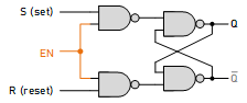
NAND Type SR Latch
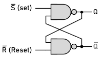
SR Latch with NAND gates
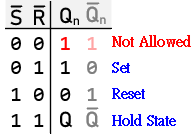
Characteristic Table

NAND-based SR Latch
- Structure: Consists of two cross-coupled NAND gates.
- Inputs Active Low: Both S and R inputs are active low due to the nature of NAND logic. This means that the normal state of S and R is high (1), and to activate an input, it must be brought low (0).
- Set Condition: To set Q to 1, S is taken low while R remains high.
- Reset Condition: To reset Q to 0, R is taken low while S remains high.
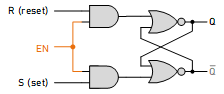
NOR Type SR Latch
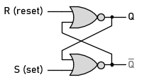
SR Latch with NOR gates
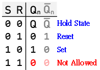
Function Table

NOR-based SR Latch
- Structure: Comprises two cross-coupled NOR gates.
- Inputs Active High: In this case, the S and R inputs are active high, aligning with the typical SR latch operation description.
- Set Condition: To set Q to 1, S is taken high while R remains low.
- Reset Condition: To reset Q to 0, R is taken high while S remains low.
Gated SR Latch — SR Latch with Control Input

Applications and Limitations
- The SR latch is used in digital circuits for simple storage tasks, such as storing a single bit of state information.
- It is a building block for more complex memory devices like flip-flops, counters, and registers.
- The major limitation is the forbidden state (both inputs high for NOR-based, or both low for NAND-based), which must be managed carefully in digital designs.
J K Latch
The JK latch is a type of sequential logic circuit, one of the fundamental building blocks in digital electronics. It's a bistable multivibrator, meaning it has two stable states that it can maintain indefinitely until triggered to switch. The JK latch expands on the functionality of simpler latches like the SR latch by resolving the ambiguous output state when both inputs are high.
Components of a JK Latch:
A basic JK latch can be constructed using NAND gates or NOR gates.


Characteristic Table of JK Latch
Circuit Description:
The JK latch consists of two cross-coupled NAND gates. Each output of a NAND gate is connected to one of the inputs of the other NAND gate. The J and K inputs are analogous to the S (set) and R (reset) inputs of an SR latch.
Inputs:
- J (Set Input): Setting this input high while the active EN sets the latch, driving the output Q to high.
- K (Reset Input): Setting this input high while the active EN resets the latch, driving the output Q to low.
- EN (optional in some configurations): Controls when the latch can change states. Changes to the output occur on the triggering level of the EN.
Behavior:
The JK latch operates with the following input conditions:
- J = 0, K = 0: No change. The latch retains its previous state.
- J = 0, K = 1: Reset. The output Q is set to low, and Q is set to high.
- J = 1, K = 0: Set. The output Q is set to high, and Q is set to low.
- J = 1, K = 1: Toggle. The output Q toggles to the opposite state (i.e., if Q is high, it becomes low, and vice versa).
D Latch
...
T Latch
...
7.3 Flip-Flops
J K Latch
...
D Latch
...
T Latch
...
7.4 Flip-Flop Conversion
Terminologies
Truth Table
- A truth table provides a complete listing of all possible input combinations and their corresponding output values for a combinational logic circuit.
- It covers all possible input states and shows the resulting output based on the logic function implemented by the circuit.
- Truth tables are commonly used for analyzing and designing combinational circuits, such as logic gates.
- Shows the relationship between inputs and outputs for all possible input combinations.
- It's the most fundamental table, like a dictionary lookup for a circuit's output based on the inputs.
Function Table
- A function table is essentially the same as a truth table.
- Applies to combinational circuits only.
- It can be used interchangeably with a truth table in many cases.
- May use different terminology for inputs and outputs (e.g., Input1, Output) compared to a truth table (A, B, F).
Characteristic Table
- A characteristic table (also known as a state table) describes the behavior of sequential circuits (e.g., flip-flops, registers).
- Shows the relationship between the circuit's current state, inputs, and next state.
- It may additionally include the output produced in the current state.
- It describes how the circuit's memory (state) changes based on inputs and how it affects the next output.
Excitation Table
- The excitation table is derived from the characteristic table.
- Applies to sequential circuits only (circuits with memory).
- Shows the input values required to transition the circuit from its current state to the next state.
- It helps design the control logic for flip-flops (circuits that store state) to achieve the desired behavior.
State Diagram
- Graphical representation of state table: these diagrams show states as nodes and transitions as directed arcs. They help visualize the behavior of the circuit over time.
State Table
- These tables list all possible states of the circuit and show the transitions between these states based on input values.
- Also called the transition table.
Here's a table summarizing the key differences:
| Feature | Truth Table / Function Table | Excitation Table | Characteristic Table | State Diagram | State table |
|---|---|---|---|---|---|
| Circuit Type | Combinational & Sequential (Truth Table) | Sequential Only | Sequential Only | Sequential Only | Sequential Only |
| Focus | Inputs & Outputs | Inputs for Next State | Current State, Inputs, Next State (and possibly Output) | Visual representation of state transitions | Tabular representation of state transitions |
| Information Provided | Output for each input combination | Inputs to cause a state transition | State transitions and possibly output | Graphical flow of states based on inputs | Tabular listing of next state and output for each state-input combination |
Analogy:
- Think of a truth table/function table as a simple instruction manual - if you give it these inputs, you get this output.
- An excitation table is like a recipe for changing state in a sequential circuit - use these inputs with the current state to get the desired next state.
- A characteristic table is like a detailed record of how a sequential circuit behaves - it shows how the state changes based on inputs and what the output is at each step.