Lesson 05: Combination Logic Circuits
5.1 Analysis of Combinational Circuits
Definition of Combinational Circuits
- Combinational circuits are digital circuits where the output at any given time depends only on the current combination of input values.
\(output = F(inputs)\) - These circuits have no memory or feedback; the output is solely determined by the current input values.
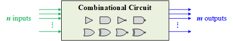
Figure 1: Block Diagram of Combinational Circuit
Basic Components of Combinational Circuits
- Logic Gates: Combinational circuits are constructed using basic logic gates such as AND, OR, NOT, NAND, NOR, XOR, and XNOR gates.
- Boolean Functions: The behavior of combinational circuits is described using Boolean functions, which express the relationship between inputs and outputs.
Design Process of Combinational Circuits
- Specification: Clearly define the inputs and outputs of the circuit and the desired behavior.
- Truth Table: Construct a truth table that lists all possible input combinations and their corresponding output values.
- Boolean Expression: Derive Boolean expressions for each output based on the truth table.
- Logic Diagram: Use the Boolean expressions to create a logic diagram consisting of interconnected logic gates.
- Verification: Simulate the circuit to ensure that it produces the correct output for all input combinations.
Examples of Combinational Circuits
- Adders: Combinational circuits that perform the addition of binary numbers.
- Subtractors: Circuits that perform subtraction by adding the two's complement of the subtrahend to the minuend.
- Multiplexers (MUX): Circuits that select one of several input data lines and direct it to the output.
- Demultiplexers (DEMUX): Circuits that take a single input and direct it to one of several output lines.
- Encoders and Decoders: Circuits that convert between different data formats, such as binary and Gray code.
- Comparators: Circuits that compare two binary numbers and determine their relationship (equal, greater than, less than).
Applications of Combinational Circuits
- Combinational circuits are used in various digital systems, including arithmetic units, data processing units, control units, and multiplexers/demultiplexers.
- They are essential building blocks for designing more complex digital systems and processors.
Combinational circuits play a crucial role in digital logic design, providing the basis for processing and manipulating digital data. Understanding their principles, design methods, and applications is essential for anyone working in the field of digital systems and computer engineering.
5.2 Binary Adder-Subtractor
Half-Adder
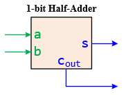
The design of a Half Adder is an introductory yet fundamental exercise in Digital Logic Design, showcasing how basic logic gates can be used to perform arithmetic operations. A Half Adder is a combinational circuit that adds two single binary digits (bits) and produces a sum and a carry output. It is called a "half" adder because it does not account for carrying inputs from previous operations, a function handled by a Full Adder. Here, we will break down the design process of a Half Adder step by step.
Define the Problem
The objective is to design a circuit that accepts two binary inputs, referred to as a and b, and produces two outputs:
- Sum (s): The result of the addition of a and b.
- Carry (cout): The carry value if the addition of a and b exceeds 1.
Design Steps:
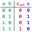
Step 1: Derive the Truth Table
Start by creating a truth table that lists all possible combinations of the input bits a and b, along with the corresponding Sum and Carry outputs.
Step 2: Determine the Logic Expressions
From the truth table, deduce the logic expressions for Sum and Carry. The expressions can be directly inferred based on the outputs:
- Sum (s) can be seen to follow the XOR pattern: s = a ⊕ b
- Carry (cout) follows the AND pattern: cout = a ⋅ b
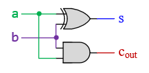
Step 3: Implement the Circuit Using Logic Gates
Based on the logic expressions derived, you can now draw the circuit:
Full-Adder
A 1-bit full-adder is a digital circuit that performs the addition of three binary digits: two significant bits and an incoming carry bit. It's an extension of the half-adder, capable of handling the carry input from a previous addition. The full adder has three inputs: a, b, and Carry-in (cin), and two outputs: Sum (s) and Carry-out (cout). The Sum output represents the least significant bit of the addition of a, b, and cin, while Carry-out represents an overflow into the next most significant bit.
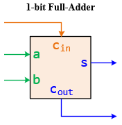
Objectives of a 1-bit Full-Adder:
- Sum (s) Output: The output should be the sum of a, b, and cin modulo 2.
- Carry-out (cout) Output: The output should be 1 if the sum of a, b, and cin is greater than or equal to 2, indicating a carry to the next higher bit.
Design Steps:
Step 1: Derive the Truth Table
Create a truth table that lists all possible combinations of the inputs a, b, and cin, along with the corresponding Sum (s) and Carry-out (cout) outputs.
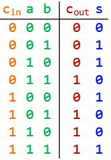
Step 2: Determine the Logic Expressions
From the truth table, deduce the logic expressions for Sum and Carry-out:
- Sum (s): This can be achieved through the equation: s = a ⊕ b ⊕ cin
- Carry-out (cout): This is a bit more complex, as cout is 1 in three cases: cout = a⋅b + b⋅cin + a⋅cin
Step 3: Implement the Circuit Using Logic Gates
Given the logic expressions, the full-adder circuit can be constructed with:
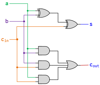
The 1-bit full-adder is essential for constructing arithmetic logic units (ALUs) and multi-bit adders, which are core components of computer processors and digital systems. Understanding its design and operation is crucial for students and engineers working in digital logic and computer architecture, enabling the creation of more complex computational devices.
Redesigning the 1-bit full adder using fewer gates
Redesigning a 1-bit full-adder to use fewer gates without compromising its functionality requires a clever approach to minimize the hardware while ensuring it still performs the necessary addition of three binary digits (two significant bits and one carry bit). The standard 1-bit full-adder circuit typically uses two XOR gates, two AND gates, and one OR gate. The goal of the redesign is to reduce the total number of gates or to use gates in a more efficient configuration.
Redesigned Full-Adder Using Fewer Gates
Redesigning the 1-bit full adder using a 1-bit half adder
...
Overflow
Binary Adder/Subtractor
5.3 Decimal Adder
5.4 Binary Multiplier
5.5 Binary Divider
5.6 Combinational Logic Circuit Design
The design procedure for combinational logic circuits starts with the problem specification and comprises the following steps:
- Determine the required number of inputs and outputs from the specifications.
- Derive the truth table for each output based on their relationships to the input.
- Simplify the boolean expression for each output. Use Karnaugh Maps or Boolean algebra.
- Draw a logic diagram that represents the simplified Boolean expression.
- Verify the design by analyzing or simulating the circuit.
5 or more
Design a circuit that has a 3-bit binary input and a single output (Z) specified as follows:
- Z = 0, when the input is less than (5)10
- Z = 1, otherwise
BCD to 7-Segment Decoder
Design a BCD to 7-segment decoder circuit for an seven-segment display that has a 4-bit binary input and seven output (seg-a, -b, -c, -d, -e, -f, and -g) specified by the truth table.
Odd Numbers
Design a circuit that has a 3-bit binary input B2, B1, and B0 (where B2 is MSB and B0 is LSB) and a single output (Z) specified as follows:
- Z = 0, even numbers
- Z = 1, odd numbers 1, 3, 5, 7
Bank Alarm System
A bank wants to install an alarm system with movement sensors. The bank has three sensors (A, B, C).
The alarm will be triggered only when at least two sensors activate simultaneously to prevent false alarms produced by a single sensor activation.
Car Safety Buzzer
Turn On the B(uzzer) whenever the D(oor) is Open OR when the K(ey) is in the Ignition AND the S(eat belt) is NOT Buckled. The logic values for each component are as below:
- 0 : Seat Belt is NOT Buckled
1 : Seat Belt is Buckled - 0 : Key is NOT in the Ignition
1 : Key is in the Ignition - 0 : Door is NOT Open
1 : Door is Open - 0 : Buzzer is OFF
1 : Buzzer is ON
Prime Numbers
Design a circuit that has a 3-bit binary input and a single output (Z) specified as follows:
- Z = 0, non prime number
- Z = 1, prime numbers 2, 3, 5, 7
1-bit Half Adder
The half-adder adds two one-bit binary numbers, A and B. The output is the Sum (S) of the two bits and the Carryout (Cout).
{Cout, S} = A + B
1-bit Full Adder
For a full adder, besides the two inputs bits A and B, the Carry in (Cin) bit is included. The outputs are Sum (S) and Carryout (Cout).
{Cout, S} = A + B + Cin
1-bit Half Subtractor
The half-subtractor subtracts two one-bit binary numbers, A and B. It produces the Difference (D) between the two input binary bits, and also produces an output Borrow (Bout) bit that indicates if one has been borrowed. In the subtraction (A - B), the A is called a Minuend bit, and the B is called a Subtrahend bit.
{Bout, D} = A - B
1-bit Full Subtractor
The half-subtractor has three inputs and two outputs. The inputs are A, B, and Bin, which denote the minuend, subtrahend, and previous borrow, respectively. The outputs are D and Bout, which re[resemt the difference and output borrow, respectively.
{Bout, D} = A - B - Bin
2-bit Comparator
Design a circuit that compares two 2-bit unsigned numbers, (A1, A0) and (B1, B0), providing three outputs such that
- LT = 1, if A1A0 < B1B0
- EQ = 1, if A1A0 = B1B0
- GT = 1, if A1A0 > B1B0
2-bit Multiplier
Design a circuit that multiplies two 2-bit unsigned numbers, (A1, A0) and (B1, B0), providing four outputs P3P2P1P0.
(A1, A0) × (B1, B0) = (P3P2P1P0)