Lesson 13: Finite State Machines (FSM)
- FSM = state + transitions + outputs. It is the standard way to model control logic in digital systems (protocols, controllers, UI flows, sequencing).
- Moore: output depends only on state → stable outputs, usually 1 clock later.
- Mealy: output depends on state + input → faster response, sometimes fewer states, but more sensitive to input glitches.
- Typical Verilog structures: 3-tier (clearest), 2-tier (compact), 1-tier (shortest but harder to maintain).
- Quartus: You must do Pin Assignments; you should add a minimal SDC create_clock for meaningful timing analysis.
13.1 Fundamentals of Finite State Machines
What is a Finite State Machine (FSM)?
A Finite State Machine (FSM) is a formal model used to describe and implement sequential control logic in digital systems. An FSM has a finite set of states, a state register that stores the current state, and logic that determines how the system moves between states. In a synchronous FSM, the next state is computed by combinational next-state logic as a function of the current state and inputs, and the state register updates to the next state on each active clock edge. Outputs are generated either from the state only (Moore FSM) or from the state and inputs (Mealy FSM).
- State: the current mode of the system (e.g., IDLE, RUN, ERROR).
- Transition: the condition for moving from one state to another.
- State Register: flip-flops holding the current state (updated on a clock edge).
- Next-State Logic: combinational logic that computes
next_state. - Output Logic: logic that computes outputs (Moore or Mealy rules).
Why is FSM important in digital circuit design?
FSMs are fundamental building blocks in digital design. They are important because:
- Structured Approach: FSMs provide a disciplined, methodical way to design control logic. Complex behavior is broken into a finite set of clearly defined states.
- Predictable Timing: Being synchronous (clocked), FSMs behave deterministically and meet timing constraints reliably on FPGAs and ASICs.
- Synthesis-Friendly: FSMs described in Verilog are well-understood by synthesis tools (such as Quartus Prime), which can automatically optimize state encoding and logic.
- Debugging Ease: The state variable provides a direct window into the machine's behavior, making simulation and hardware debugging straightforward.
- Scalability: Complex systems can be built by interconnecting multiple FSMs (Hierarchical FSMs), keeping each module manageable.
- Universality: Every digital controller—from a simple LED blinker to a full USB protocol stack—can be modeled as an FSM.
💡Key Takeaway
If your circuit needs to remember what happened before and make decisions based on that history, you need an FSM.
When to Use an FSM
Deploy an FSM whenever a system requires:
- Sequence execution (e.g., initialization sequences and communication protocols such as I2C and SPI).
- State-dependent outputs (e.g., traffic light controllers, vending machines).
- Control path logic to coordinate datapaths.
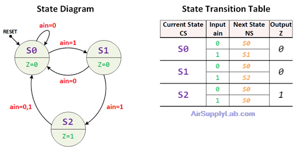
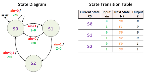
State Diagrams
A state diagram (also called a state transition diagram) is a visual representation of an FSM. It uses state nodes and transition arrows. Each transition is labeled with a condition. In Moore FSMs, outputs are typically labeled on the inside of states. In Mealy FSMs, outputs are often labeled on transitions as condition/output.
State Diagram Components
| Symbol | Represents | Description |
|---|---|---|
| State | Each circle represents one state. The state name is written inside. | |
| Initial State | An arrow pointing into the circle indicates the reset/initial state. | |
| Transition | Directed arrow from one state to another, labeled with condition(s). | |
| Label on arrow | Condition/Output | Moore: input only. Mealy: input/output. |
| Self Transition | The FSM stays in the same state under this condition. |
State Transition Table
A State Transition Table is a tabular representation of an FSM. It explicitly lists every combination of current state and input, and specifies the next state (and output) for each combination.
Is the State Transition Table useful in Verilog? — Yes, absolutely!
While a state diagram gives a visual overview, the state transition table provides the precise logic needed to write Verilog case statements. Every row in the table maps directly to a case / if condition in the next-state always block.
- Enumerate every state/condition combination to avoid missing corner cases.
- Map cleanly into case(curState) for next-state logic.
- Build self-check testbenches (the table becomes your golden reference).
✅ Practical Rule
Build the state transition table BEFORE writing Verilog. It prevents logic errors and ensures complete coverage of all state/input combinations. Synthesis tools use this same logic internally.
Moore State Diagram
In a Moore machine, outputs are associated with STATES (written inside or below the circle). Transition labels show only the input condition.
Output is labeled INSIDE / BELOW each state
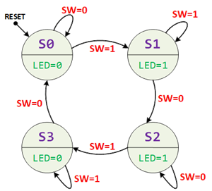
Transition Labels: Input condition ONLY (SW=0 or SW=1)
Output Labels: Written INSIDE/BELOW each state circle
Figure 1: Moore FSM State Diagram — LED Toggle Example
State Transition Table for the LED Toggle FSM (Moore):
| Current State | Input (SW) | Next State | Output (LED) |
| S0 | 0 | S0 | OFF |
| 1 | S1 | ||
| S1 | 0 | S2 | ON |
| 1 | S1 | ||
| S2 | 0 | S2 | ON |
| 1 | S3 | ||
| S3 | 0 | S0 | OFF |
| 1 | S3 |
Timing Diagram:
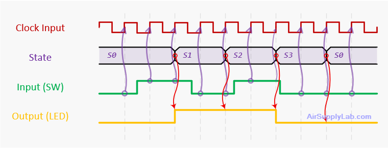
Figure 2: Moore timing (output follows registered state; often 1-cycle later)
Mealy State Diagram
In a Mealy machine, outputs are associated with TRANSITIONS (labeled Input/Output on the arrows). The output can change as soon as the input changes, even before the next clock edge.
Output is labeled ON THE TRANSITION ARROW
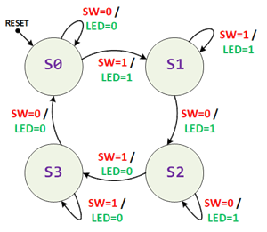
Transition Labels: Input/Output (e.g., SW=1 / LED=1)
State Circles: No output inside (unlike Moore)
Figure 3: Mealy FSM State Diagram — LED Toggle Example
State Transition Table for the LED Toggle FSM (Mealy):
| Current State | Input (SW) | Next State | Output (LED) |
| S0 | 0 | S0 | OFF |
| 1 | S1 | ON | |
| S1 | 0 | S2 | ON |
| 1 | S1 | ON | |
| S2 | 0 | S2 | ON |
| 1 | S3 | OFF | |
| S3 | 0 | S0 | OFF |
| 1 | S3 | OFF |
Timing Diagram:
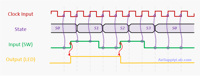
Figure 4: Mealy Timing (output can change in the same cycle)
Types of FSM: Moore and Mealy:
| Characteristic | Moore FSM | Mealy FSM |
|---|---|---|
| Output depends on | Current state only | Current state + inputs |
| State diagram labels | Output inside/below state node | Output on transition arrow (in/out) |
| Number of states | More states required | Fewer states (often 1 less per output) |
| Output glitches | Glitch-free (registered output) | Possible if inputs are noisy |
| Response speed | Output changes 1 cycle after input | Output can change same cycle as input |
| Typical use | Safe, registered outputs for FPGAs | Fast response, fewer states |
13.2 Moore and Mealy FSM Models
Types of FSM:
- Moore Machine: Outputs depend only on the current state.
- Mealy Machine: Outputs depend on both the current state and the current inputs.
The Moore FSM
Understanding Moore FSM
A Moore Finite State Machine is an FSM where the OUTPUTS are a function of the CURRENT STATE ONLY. The inputs only affect what the next state will be — they do not directly affect the output.
This means output changes happen only at clock edges (when the state register updates), making Moore outputs inherently registered and glitch-free. This property is highly desirable in FPGA designs.
Moore FSM characteristics
- Stable outputs (outputs depend only on the registered state).
- Often 1-cycle latency: input → next_state → state update (clock edge) → output update.
- Good for outputs that must be glitch-free (chip enables, control strobes, critical control signals).
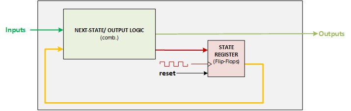
Moore FSM Block Diagram
A Moore FSM consists of three logical blocks:
- Next-State Logic: Combinational logic. Takes current state and inputs → computes next state.
- State Register: Sequential logic (flip-flops). Stores the current state. Updates on the clock edge.
- Output Logic: Combinational logic. Takes only the current state → produces outputs.
MOORE FSM — BLOCK DIAGRAM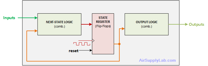
Figure 5: Moore FSM Block Diagram (3-Block Architecture)
The Mealy FSM
Understanding Mealy FSM
A Mealy Finite State Machine is an FSM in which the OUTPUTS are a function of BOTH the current state AND the current inputs. The output can change as soon as the input changes, without waiting for the next clock edge.
This means Mealy machines can respond faster (in the same clock cycle as the input), and often require fewer states than an equivalent Moore machine. However, the outputs may exhibit glitches if the inputs change unpredictably.
Mealy FSM characteristics
- Fast response: output can change in the same cycle as input changes (combinational output).
- Potentially fewer states than Moore for some behaviors.
- More sensitive to glitches: inputs must be synchronized/debounced to avoid unstable outputs.
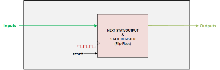
Mealy FSM Block Diagram
Like Moore, a Mealy FSM also consists of three logical blocks, but the Output Logic receives both the current state AND the inputs:
- Next-State Logic: Combinational logic. Takes current state and inputs → computes next state.
- State Register: Sequential logic (flip-flops). Stores the current state. Updates on the clock edge.
- Output Logic: Combinational logic. Takes current state AND inputs → produces outputs.
MEALY FSM — BLOCK DIAGRAM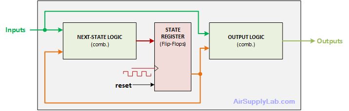
Figure 6: Mealy FSM Block Diagram (3-Block Architecture)
Moore vs. Mealy: Comparison
Key Differences
| Aspect | Moore FSM | Mealy FSM |
|---|---|---|
| Output definition | Output = f(Current State) | Output = f(Current State, Input) |
| State diagram label | Output inside/below state node | Output on transition arrow (in/out) |
| Number of states | More states required | Fewer states needed |
| Output glitches | Glitch-free (registered output) | Possible if inputs are noisy |
| Response speed | 1 cycle after input | Same cycle as input |
| Initial output | Defined by the initial state | Depends on the state and current input |
Timing of Output
This is one of the most critical differences. Consider a simple sequence where the input goes HIGH at clock cycle N:
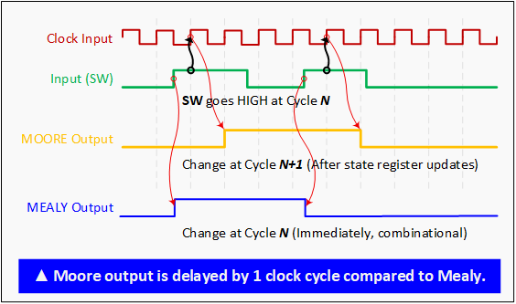
Figure 7: Moore vs. Mealy Output Timing Comparison
Complexity and Efficiency
State Count: Mealy machines typically require one fewer state than Moore FSMs for the same behavior, because Mealy machines can produce output during a transition rather than requiring an intermediate state.
Logic Complexity: Mealy output logic is more complex (depends on both state and input), but the reduced state count can result in fewer flip-flops. Moore has simpler output logic but may need more states.
FPGA Resource Usage: For most practical MAX-10 designs, both types use comparable LUT counts. Moore is generally preferred because registered outputs reduce timing concerns.
Applications in Digital Circuits
| Application | Preferred FSM | Reason |
|---|---|---|
| LED / Relay control | Moore | Stable, glitch-free registered output |
| Sequence detector | Mealy | Fewer states, faster recognition |
| UART / SPI protocol | Mealy | Output response needed in the same cycle |
| Traffic light controller | Moore | Clean, synchronous output transitions |
| Debounce logic | Moore | Output stability is a priority |
| Handshake / ACK signals | Mealy | Immediate response to a valid signal |
| Game controller logic | Moore | Predictable state-based outputs |
13.3 FSM Design Methodology (State Diagram → Table → RTL)
13.3 FSM Design Methodology (State Diagram → Table →RTL)
A finite-state machine should not be written directly in Verilog without planning. A correct FSM design usually follows a structured process:
Problem Description → State Diagram → State Table → State Encoding → Verilog Code → Simulation Verification.
This design flow helps students move from system behavior to synthesizable RTL code in a clear and systematic way.
1. Problem Description
1. Start from the Problem Specification
Before drawing any state diagram, define the system's required behavior. The designer should clearly identify:
- What the inputs are
- What the outputs are
- What events cause state transitions
- What the initial state should be
- Whether the output depends only on the current state or on both the state and the inputs
At this stage, the goal is not to write Verilog yet. The goal is to understand what the circuit is supposed to do.
For example, in a sequence detector, the designer should determine:
- What bit pattern should be detected
- Whether overlapping detection is allowed
- When the output should be asserted
- Whether the machine should be Moore or Mealy
2. State Diagram
2. Draw the State Diagram
Once the behavior is clear, the next step is to draw the state diagram. A state diagram is a graphical representation of the FSM. It shows:
- All states in the machine
- The transition conditions between states
- The output behavior of each state or transition
This is the most important planning step because it converts the verbal problem into a formal machine model.
For a Moore FSM, outputs are associated with states. Each state bubble usually includes the output value.
For a Mealy FSM, outputs are associated with transitions. Each transition label usually includes input/output notation.
A good state diagram should satisfy the following:
- Every state has a clear meaning
- Every possible input condition is covered
- No transition is ambiguous
- The reset or initial state is clearly identified
3. State Table
3. Convert the State Diagram into a State Table
After the state diagram is complete, convert it into a state table. A state table lists the behavior in a tabular form, which is often easier to translate into code.
A typical state table includes:
- present state,
- input condition,
- next state,
- output.
| Present State | Input | Next State | Output |
|---|---|---|---|
| S_IDLE | 0 | S_IDLE | 0 |
| S_IDLE | 1 | S_START | 0 |
| S_START | 0 | S_IDLE | 0 |
| S_START | 1 | S_WAIT | 0 |
| S_WAIT | 0 | S_DONE | 0 |
| S_WAIT | 1 | S_DONE | 0 |
| S_DONE | 0 | S_IDLE | 0 |
| S_DONE | 1 | S_IDLE | 1 |
The state table helps students check whether:
- All transitions are covered
- Any cases are missing
- Outputs are assigned correctly
- The FSM behavior matches the state diagram
4. State Encoding
4.1. Choose State Names and State Encoding
After the state behavior is defined, assign symbolic names to the states. Examples include: S_IDLE, S_START, S_WAIT, and S_DONE.
These symbolic names make the code much easier to read than raw binary values.
Then assign binary values to each state:
localparam S_IDLE  = 2'b00;
localparam S_START = 2'b01;
localparam S_WAIT  = 2'b10;
localparam S_DONE  = 2'b11;
At the teaching level, students usually use simple binary encoding first. Later, more advanced topics may discuss one-hot encoding, Gray encoding, or synthesis-selected encoding.
4.2. Separate the FSM into Standard Design Blocks
Before coding, students should understand that an FSM is usually divided into three logical parts:
(1) State Register
The state register stores the current state. This is sequential logic.
always @(posedge clk) begin
    if (rst)
        state <= IDLE;
    else
        state <= next_state;
end
(2) Next-State Logic
The next-state logic calculates the next state from the current state and inputs. This is combinational logic.
always @(*) begin
    case (state)
        S_IDLE: begin
            if (x)
                next_state = S_START;
            else
                next_state = S_IDLE;
        end

        ...

        default: next_state = S_IDLE;
    endcase
end
(3) Output Logic
The output logic generates the outputs. For a Moore FSM, the output depends only on the current state. For a Mealy FSM, the output depends on both the current state and the inputs.
This separation is important because it keeps RTL code clean and prevents mixing combinational and sequential behavior.
5. Verilog Code
5.1. Write the Verilog Code Systematically
After the planning is complete, write the code in the following order:
Step 1: Declare Inputs, Outputs, and Internal State Variables
module fsm_example (clk, rst, x, y);
    input  clk;
    input  rst;
    input  x;
    output y;

    reg    y;
    reg [1:0] state, next_state;
Step 2: Define State Encodings
localparam S_IDLE  = 2'b00,
           S_S1    = 2'b01,
           S_S2    = 2'b10,
           S_DONE  = 2'b11;
Step 3: Write the State Register Block
always @(posedge clk) begin
    if (rst)
        state <= IDLE;
    else
        state <= next_state;
end
Step 4: Write the Next-State Logic Block
always @(*) begin
    next_state = IDLE;

    case (state)
        S_IDLE: begin
            if (x)
                next_state = S1;
            else
                next_state = S_IDLE;
        end

        S_S1: begin
            if (x)
                next_state = S_S2;
            else
                next_state = S_IDLE;
        end

        S_S2: begin
            next_state = S_DONE;
        end

        S_DONE: begin
            next_state = S_IDLE;
        end

        default: next_state = S_IDLE;
    endcase
end
Step 5: Write the Output Logic Block
For a Moore FSM:
always @(*) begin
    case (state)
        S_DONE:  y = 1'b1;

        default: y = 1'b0;
    endcase
end
For a Mealy FSM:
always @(*) begin
    y = 1'b1;

    case (state)
        S_DOWN: begin
            if (x)
                y = 1'b1;
        end
    endcase
end
5.2. Verify the Code Against the State Table
After writing the code, students should compare it with the original state table. They should confirm:
- Does every state appear in the code?
- Does every input condition lead to the correct next state?
- Are outputs correct for each case?
- Is the reset state correct?
- Is there a default assignment for safety?
This step prevents many logic errors before simulation.
6. Simulation Verification
6. Simulate the FSM
FSM design is not complete until it is verified by simulation. The testbench should:
- Apply reset,
- Drive representative input sequences,
- Observe state transitions,
- Confirm output timing,
- Test both normal and corner cases.
For example, the simulation should check:
- Startup after reset,
- Valid transitions,
- Invalid or unexpected input cases,
- Correct output timing,
- Return to S_IDLE when required.
Common Mistakes in FSM Methodology
Students often make the following mistakes:
- Writing code before drawing the state diagram.
- Incomplete next-state logic.
- No default assignment.
- Mixing next-state logic and state register logic.
- Incorrect output logic placement.
- Missing reset state.
These problems often lead to incomplete transitions, latch inference, or incorrect simulation results.
Recommended FSM Design Workflow
A good practical rule is:
Do not start with Verilog code.
Start with the behavior, then draw the state diagram, convert it to a state table, and write the RTL code only then.
This design discipline produces cleaner FSMs and makes debugging much easier.
Summary
FSM design should follow a structured and repeatable process: State Diagram → State Table → State Encoding → RTL Code → Simulation.
This methodology helps students:
- understand the system behavior before coding,
- organize the FSM clearly,
- write cleaner Verilog,
- avoid common mistakes,
- and verify the design systematically.
For both Moore and Mealy machines, this design flow is more important than memorizing code templates. A well-designed FSM begins with a clear model, not with random code writing.
13.4 Implementing a Moore FSM in Verilog
Moore FSM Lab: "Two-Consecutive-High" Detector with a One-Cycle Pulse Output
Introduction
This document presents a structured, engineering-oriented guide to implementing a Moore finite state machine (FSM) in Verilog HDL using three widely used coding styles: 3-tier, 2-tier, and 1-tier. The purpose is not to provide a laboratory procedure, but to demonstrate how the same behavioral specification can be mapped into different RTL organizations, and to clarify the practical trade-offs in readability, maintainability, and verification.
As a running example, we implement a synchronous “two-consecutive-high” detector: when the input ain is asserted for two consecutive clock cycles, the circuit generates a single-clock-cycle pulse on output z; otherwise, z remains low. The FSM is designed as a Moore machine, meaning the output is determined solely by the current state. This example is intentionally small (three states) so that the structural differences among the three implementation styles are easy to see and compare.
Inputs and Outputs
- Inputs:
- clk : system clock
- rst_n : active-low reset
- ain : 1-bit input signal
- Output:
- z : 1-bit output pulse
Functional Specification
- If ain is high for two consecutive clock cycles, then output z becomes high for exactly one clock cycle (one-cycle pulse).
- In all other cases, z = 0.
- The design must be a Moore FSM (output depends only on the current state).
You will implement the same Moore FSM using three Verilog HDL coding styles:
- 3-tier (3 always blocks)
- 2-tier (2 always blocks)
- 1-tier (1 always block)
3-Tier Moore Implementation (3 always blocks)
3-Tier Implementation (3 always blocks)
The 3-tier style is the most recommended. It separates three concerns into three always blocks:
- Block A: always @(*) for Next-State Logic (combinational)
- Block B: always @(posedge clk or negedge rst_n) for the State Register (sequential, clocked)
- Block C: always @(*) for Moore Output Logic (z = f(curState), combinational)
fsm_pulse_3tier / Verilog
// =====================================================================================
// Moore FSM — 3-Tier / 3-Always Block Style
// =====================================================================================
// Description : Two-Consecutive-High Detector with a One-Cycle Pulse Output (Moore FSM)
// Synthesizer : Altera Quartus Prime V2x
// Platform    : Intel Altera MAX-10 FPGA
// =====================================================================================
module fsm_pulse_3tier (clk, rst_n, ain, z);
    input  clk;
    input  rst_n;
    input  ain;
    output z;

    // State encoding (2 bits is enough for 3 states)
    parameter S0 = 2'b00;
    parameter S1 = 2'b01;
    parameter S2 = 2'b10;

    reg [1:0] currState;
    reg [1:0] nextState;
    reg       z;
//----------------------------------------------------------------------------------
    // A) Next-state logic (combinational)
    always @(*) begin
        nextState = currState; // default
        case (state)
            S0: begin
                if (ain) nextState = S1;
                else     nextState = S0;
            end
            S1: begin
                if (ain) nextState = S2;
                else     nextState = S0;
            end
            S2: begin
                nextState = S0; // regardless of ain
            end
            default: begin
                nextState = S0;
            end
        endcase
    end
//----------------------------------------------------------------------------------
    // B) State register (sequential)
    always @(posedge clk or negedge rst_n) begin
        if (!rst_n)
            currState <= S0;
        else
            currState <= nextState;
    end
//----------------------------------------------------------------------------------
    // C) Output logic (Moore: z depends only on currState)
    always @(*) begin
        case (currState)
            S0: z = 1'b0;
            S1: z = 1'b0;
            S2: z = 1'b1;
            default: z = 1'b0;
        endcase
    end
endmodule
Testbench
This testbench verifies the expected timing of the 3-tier/2-tier Moore structure (where z is driven by the current state).
Testbench / Verilog
`timescale 1ns/1ps

module fsm_pulse_tb();

    reg     clk;
    reg     rst_n;
    reg     ain;
    wire    z;

    // Select one DUT
    fsm_pulse_3tier DUT (.clk(clk), .rst_n(rst_n), .ain(ain), .z(z));
 // fsm_pulse_2tier DUT (.clk(clk), .rst_n(rst_n), .ain(ain), .z(z));
 // fsm_pulse_1tier DUT (.clk(clk), .rst_n(rst_n), .ain(ain), .z(z));

    // 10ns clock period
    initial clk = 1'b0;
    always #5 clk = ~clk;
//----------------------------------------------------------------------------------
    // Apply ain for N cycles (update at negedge to avoid race)
    task apply_ain;
        input val;
        input integer cycles;
        integer i;
        begin
            for (i = 0; i < cycles; i = i + 1) begin
                @(negedge clk);
                ain = val;
            end
        end
    endtask
//----------------------------------------------------------------------------------
    // Expected z for 3-tier/2-tier Moore FSM:
    // z(k) = 1 if ain was 1 in BOTH of the two previous sampled cycles.
    reg ain_d1, ain_d2;
    reg expected_z;

    always @(posedge clk or negedge rst_n) begin
        if (!rst_n) begin
            ain_d1     <= 1'b0;
            ain_d2     <= 1'b0;
            expected_z <= 1'b0;
        end else begin
            ain_d2     <= ain_d1;
            ain_d1     <= ain;
            expected_z <= (ain_d2 & ain_d1);
        end
    end
//----------------------------------------------------------------------------------
    initial begin
        // init
        ain   = 1'b0;
        rst_n = 1'b0;

        // reset
        repeat (2) @(negedge clk);
        rst_n = 1'b1;

        // Test 1: all zeros
        apply_ain(1'b0, 2);

        // Test 2: single '1' only (no pulse)
        apply_ain(1'b1, 1);
        apply_ain(1'b0, 3);

        // Test 3: two consecutive '1' (one pulse)
        apply_ain(1'b1, 2);
        apply_ain(1'b0, 3);

        // Test 4: long run of '1' (pulses repeat as machine restarts)
        apply_ain(1'b1, 6);
        apply_ain(1'b0, 3);

        // Test 5: broken pattern 1,0,1,1
        apply_ain(1'b1, 1);
        apply_ain(1'b0, 1);
        apply_ain(1'b1, 2);
        apply_ain(1'b0, 3);

        $display("PASS: All tests passed.");
        $stop;
    end
endmodule
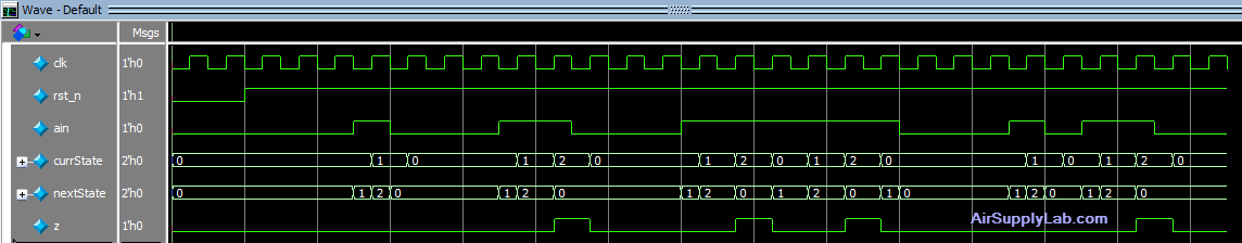
Waveform Screen Capture and Waveform Explanation
The waveform from your simulator (ModelSim/Questa/Quartus simulation) is shown below:
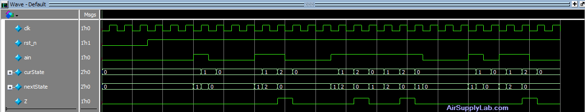
Waveform Screen Capture and Waveform Explanation
You must capture waveforms from your simulator (ModelSim/Questa/Quartus simulation). Add these signals: clk, rst_n, ain, z (add internal state if possible).
Expected waveform behavior:
- z goes high for exactly one cycle only after ain has been high for two consecutive cycles.
- After the pulse, z returns to 0.
- If ain stays high for a long time, the FSM repeats S0→S1→S2→S0, so z will periodically pulse (once per cycle when S2 is reached).
Advantages and Disadvantages
| Type | Details |
|---|---|
| ✅ Advantage | Maximum readability — each block has one clear purpose. |
| ✅ Advantage | Easiest to debug — trace next-state, state, and output separately in simulation. |
| ✅ Advantage | Industry standard — most Verilog style guides recommend this approach. |
| ✅ Advantage | Synthesis-friendly — tools can easily identify and optimize each block independently. |
| ✅ Advantage | Safe — separate always blocks reduce the risk of unintentional latches. |
| ❌ Disadvantage | Slightly more verbose — more lines of code for the same logic. |
| ❌ Disadvantage | Three always blocks can feel repetitive for very simple FSMs. |
2-Tier Moore Implementation (2 always blocks)
2-Tier Implementation (2 always blocks)
The 2-tier style merges Next-State Logic and Output Logic into a single combinational block.
- Block A: always @(*) combines next-state logic and Moore output
- Block B: always @(posedge clk or negedge rst_n) is the state register
fsm_pulse_2tier / Verilog
// ================================================================
// Moore FSM — 2-Tier / 2-Always Block Style
// ================================================================
module fsm_pulse_2tier (clk, rst_n, ain, z);
    input  clk;
    input  rst_n;
    input  ain;
    output z;

    parameter S0 = 2'b00;
    parameter S1 = 2'b01;
    parameter S2 = 2'b10;

    reg [1:0] currState;
    reg [1:0] nextState;
    reg z;

    // A) Next-state + output combined (combinational)
    always @(*) begin
        // Moore output from current state
        if (currState == S2) z = 1'b1;
        else                 z = 1'b0;

        // Next-state default
        nextState = currState;
        case (currState)
            S0: nextState = (ain) ? S1 : S0;
            S1: nextState = (ain) ? S2 : S0;
            S2: nextState = S0;
            default: nextState = S0;
        endcase
    end

    // B) State register
    always @(posedge clk or negedge rst_n) begin
        if (!rst_n)
            currState <= S0;
        else
            currState <= nextState;
    end
endmodule
Advantages and Disadvantages
| Type | Details |
|---|---|
| ✅ Advantage | More compact — fewer lines of code. |
| ✅ Advantage | Output and next-state are co-located — easy to see what each state does at a glance. |
| ✅ Advantage | Clear separation between sequential (Block 2) and combinational (Block 1) intent. |
| ❌ Disadvantage | Harder to read for large FSMs with many outputs or many states. |
| ❌ Disadvantage | Must always provide default assignments to avoid latches. |
| ❌ Disadvantage | Mixing output and next-state can cause confusion, especially for Mealy FSMs. |
1-Tier Moore Implementation (1 always block)
The 1-tier style combines ALL logic — next-state, state register, and output — into a SINGLE clocked always block.
- Set a default z <= 0 every cycle
- In S2, set z <= 1 for one cycle, and return to S0
Important: In a 1-tier style, z is typically a registered output. The behavior still meets the specification (one-cycle pulse), but the output timing is driven by the clocked block.
fsm_pulse_1tier / Verilog
module fsm_pulse_1tier (clk, rst_n, ain, z);
    input  clk;
    input  rst_n;
    input  ain;
    output z;

    parameter S0 = 2'b00;
    parameter S1 = 2'b01;
    parameter S2 = 2'b10;

    reg [1:0] state;
    reg z;

    always @(posedge clk or negedge rst_n) begin
        if (!rst_n) begin
            state <= S0;
            z     <= 1'b0;
        end else begin
            // default output each cycle
            z <= 1'b0;

            case (state)
                S0: begin
                    if (ain) state <= S1;
                    else     state <= S0;
                end
                S1: begin
                    if (ain) state <= S2;
                    else     state <= S0;
                end
                S2: begin
                    z     <= 1'b1;  // one-cycle pulse
                    state <= S0;    // return to S0 regardless of ain
                end
                default: begin
                    state <= S0;
                    z     <= 1'b0;
                end
            endcase
        end
    end
endmodule
Advantages and Disadvantages
| Type | Details |
|---|---|
| ✅ Advantage | Maximum readability — each block has one clear purpose. |
| ✅ Advantage | Easiest to debug — trace next-state, state, and output separately in simulation. |
| ✅ Advantage | Industry standard — most Verilog style guides recommend this approach. |
| ✅ Advantage | Synthesis-friendly — tools can easily identify and optimize each block independently. |
| ✅ Advantage | Safe — separate always blocks reduce the risk of unintentional latches. |
| ❌ Disadvantage | Slightly more verbose — more lines of code for the same logic. |
| ❌ Disadvantage | Three always blocks can feel repetitive for very simple FSMs. |
Comparison: 3-Tier vs. 2-Tier vs. 1-Tier (Moore)
| Criterion | 3-Tier | 2-Tier | 1-Tier |
|---|---|---|---|
| Code length | Longest | Medium | Shortest |
| Readability | Highest | Good | Lowest (large FSMs) |
| Debugging ease | Easiest | Good | Hardest |
| Latch risk | Lowest | Low (need defaults) | None (all clocked) |
| Output latency | Combinational (fast) | Combinational (fast) | Registered (+1 cycle) |
| Output glitch risk | Low | Low | None |
| Recommended for | All FSMs / complex | Small–medium FSMs | Simple FSMs only |
| Industry use | Most common | Common | Rare |
13.5 Implementing a Mealy FSM in Verilog
Mealy FSM Lab: "Two-Consecutive-High" Detector with a One-Cycle Pulse Output
Introduction
Here, explains how to implement the same “two-consecutive-high detector” as a Mealy finite state machine (FSM) using Verilog HDL. Three RTL coding organizations are presented: 3-tier, 2-tier, and 1-tier. The objective is to show how a Mealy output (a function of state and input) affects RTL structure, output timing, and verification expectations.
In a Mealy machine, outputs can change immediately with input changes (within the same clock cycle), reducing latency compared to a Moore machine. However, because outputs may depend directly on the input, the design must assume the input is synchronous (or properly synchronized) to avoid glitches.
Inputs and Outputs
- Inputs:
- clk : system clock
- rst_n : active-low reset
- ain : 1-bit input signal
- Output:
- z : 1-bit output pulse
Behavioral Requirement (Same Project Goal)
- If ain is high for two consecutive clock cycles, generate a one-clock-cycle pulse on z; otherwise, z = 0.
- Keep the same conceptual "count consecutive highs" behavior, but we implement z as a Mealy output, i.e., z = f(state, ain).
Mealy FSM Model (states and transitions)
3-Tier Mealy Implementation (3 always blocks)
3-Tier Mealy Implementation (3 always blocks)
The 3-tier style is the most recommended. It separates three concerns into three always blocks:
- Block A: always @(*) for Next-State Logic (combinational)
- Block B: always @(posedge clk or negedge rst_n) for the State Register (sequential, clocked)
- Block C: always @(*) for Mealy Output Logic (z = f(curState, ain), combinational)
fsm_pulse_3tier / Verilog
// =====================================================================================
// Mealy FSM — 3-Tier / 3-Always Block Style
// =====================================================================================
// Description : Two-Consecutive-High Detector with a One-Cycle Pulse Output (Moore FSM)
// Synthesizer : Altera Quartus Prime V2x
// Platform    : Intel Altera MAX-10 FPGA
// =====================================================================================
module fsm_mealy_pulse_3tier (clk, rst_n, ain, z);
    input  clk;
    input  rst_n;
    input  ain;
    output z;

    // State encoding
    parameter S0 = 2'b00;
    parameter S1 = 2'b01;
    parameter S2 = 2'b10;

    reg [1:0] currState;
    reg [1:0] nextState;
    reg z;
//----------------------------------------------------------------------------------
    // (1) Next-state logic (combinational)
    always @(*) begin
        case (currState)
            S0: begin
                if (ain) nextState = S1;
                else     nextState = S0;
            end
            S1: begin
                if (ain) nextState = S2; // second consecutive high
                else     nextState = S0;
            end
            S2: begin
                nextState = S0;
            end
            default: begin
                nextState = S0;
            end
        endcase
    end
//----------------------------------------------------------------------------------
    // (2) State register (sequential)
    always @(posedge clk or negedge rst_n) begin
        if (!rst_n)
            currState <= S0;
        else
            currState <= nextState;
    end
//----------------------------------------------------------------------------------
    // (3) Output logic (Mealy: depends on currState and input)
    // Pulse asserted immediately when the second '1' is observed while in S1.
    always @(*) begin
        case (currState)
            S0: z = 1'b0;
            S1: z = 1'b0;
            S2: z = 1'b1;
            default: z = 1'b0;
        endcase
    end
endmodule
Testbench
Testbench / Verilog
`timescale 1ns/1ps

module fsm_mealy_pulse_tb();
    reg   clk;
    reg   rst_n;
    reg   ain;
    wire  z;

    // Select ONE DUT:
    fsm_mealy_pulse_3tier DUT (.clk(clk), .rst_n(rst_n), .ain(ain), .z(z));
    // fsm_mealy_pulse_2tier DUT (.clk(clk), .rst_n(rst_n), .ain(ain), .z(z));
    // fsm_mealy_pulse_1tier DUT (.clk(clk), .rst_n(rst_n), .ain(ain), .z(z));

    // 10ns clock
    initial clk = 1'b0;
    always #5 clk = ~clk;
//----------------------------------------------------------------------------------
    // Apply ain on negedge to avoid race
    task apply_ain;
        input val;
        input integer cycles;
        integer i;
        begin
            for (i = 0; i < cycles; i = i + 1) begin
                @(negedge clk);
                ain = val;
            end
        end
    endtask
//----------------------------------------------------------------------------------
    // Expected z for THIS Mealy FSM:
    // z should assert when the second consecutive '1' occurs.
    // That corresponds to: ain_d1==1 AND ain==1 (current sampled cycle is second '1').
    reg ain_d1;
    reg expected_z;

    always @(posedge clk or negedge rst_n) begin
        if (!rst_n) begin
            ain_d1     <= 1'b0;
            expected_z <= 1'b0;
        end else begin
            expected_z <= (ain_d1 & ain);
            ain_d1     <= ain;
        end
    end
//----------------------------------------------------------------------------------
    initial begin
        ain   = 1'b0;
        rst_n = 1'b0;

        repeat (2) @(negedge clk);
        rst_n = 1'b1;

        // Test 1: all zeros -> no pulse
        apply_ain(1'b0, 2);

        // Test 2: single 1 -> no pulse
        apply_ain(1'b1, 1);
        apply_ain(1'b0, 3);

        // Test 3: two consecutive 1s -> one pulse on second 1
        apply_ain(1'b1, 2);
        apply_ain(1'b0, 3);

        // Test 4: long run of 1s -> pulses every other cycle (second, fourth, sixth, ...)
        apply_ain(1'b1, 6);
        apply_ain(1'b0, 3);

        // Test 5: broken pattern 1,0,1,1 -> pulse only at the end
        apply_ain(1'b1, 1);
        apply_ain(1'b0, 1);
        apply_ain(1'b1, 2);
        apply_ain(1'b0, 3);

        $display("PASS: All tests passed.");
        $stop;
    end
endmodule
Waveform Screen Capture and Explanation
You must capture waveforms in your simulator. Add signals:
- clk, rst_n, ain, currState, nextState, z
(optionally internal state/next_state)
Explain in the report:
- z asserts when the second consecutive high occurs (Mealy output reacts within the same cycle).
- For input pattern "… 1, 1 …", z becomes 1 during the second "1" cycle.
- After that, the FSM enters S2 and then re-arms based on ain.
Expected Waveform Behavior (conceptual)
- Example: ain = 0 1 1 0
z should pulse on the second '1' immediately: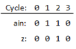
- Long run example: ain = 0 1 1 1 1 1 0
z pulses every other cycle after the first two highs: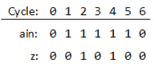
Advantages and Disadvantages
| Type | Details |
|---|---|
| ✅ Advantage | Cleanly separates next-state, state register, and output — industry best practice. |
| ✅ Advantage | Correct Mealy behavior: output is combinational (depends on input + state simultaneously). |
| ✅ Advantage | Easier to verify in simulation — each block can be inspected separately. |
| ❌ Disadvantage | Output is combinational — susceptible to glitches if sw is noisy (use debounce logic). |
| ❌ Disadvantage | Slightly more verbose than 2-tier or 1-tier styles. |
2-Tier Mealy Implementation (2 always blocks)
fsm_pulse_2tier / Verilog
// =====================================================================================
// Mealy FSM — 2-Tier / 2-Always Block Style
// =====================================================================================
// Description : Two-Consecutive-High Detector with a One-Cycle Pulse Output (Moore FSM)
// Synthesizer : Altera Quartus Prime V2x
// Platform    : Intel Altera MAX-10 FPGA
// =====================================================================================
module fsm_mealy_pulse_2tier (clk, rst_n, ain, z);
    input  clk;
    input  rst_n;
    input  ain;
    output z;

    localparam S0 = 2'b00;
    localparam S1 = 2'b01;
    localparam S2 = 2'b10;

    reg [1:0] currState;
    reg [1:0] nextState;
    reg z;

    // (1) Next-currState + output combined (combinational)
    always @(*) begin
        // Mealy output
        case (currState)
            S0: z = 1'b0;
            S1: z = 1'b0;
            S2: z = 1'b1;
        default: z = 1'b0;
        endcase

        case (currState)
            S0: nextState = (ain) ? S1 : S0;
            S1: nextState = (ain) ? S2 : S0;
            S2: nextState = S0;
            default: nextState = S0;
        endcase
    end

    // (2) currState register (sequential)
    always @(posedge clk or negedge rst_n) begin
        if (!rst_n)
            currState <= S0;
        else
            currState <= nextState;
    end

endmodule
Testbench
Reuse the same testbench as in the 3-tier section; just switch the DUT instance.
Waveform + Expected Behavior
Should match 3-tier, because both implement the same Mealy equations.
Advantages and Disadvantages
| Type | Details |
|---|---|
| ✅ Advantage | Compact — fewer always blocks while maintaining correct Mealy behavior. |
| ✅ Advantage | Transition and output are co-located — easy to see what happens in each state/input combination. |
| ✅ Advantage | Default assignments prevent latches. |
| ❌ Disadvantage | Mixing next-state and output can make large FSMs harder to read. |
| ❌ Disadvantage | Still has combinational output — glitch risk from noisy inputs. |
1-Tier Mealy Implementation (1 always block)
⚠️ Important Warning
A true Mealy FSM should NOT be implemented in a single clocked always block, because the Mealy output must be COMBINATIONAL. If you put everything in a clocked block, the output becomes registered (making it behave like a Moore machine). The example below shows a Registered Mealy variant — use it only when glitch-free output is more important than immediate response.
fsm_pulse_1tier / Verilog
// ================================================================
// Mealy FSM — 1-Tier / 1-Always Block Style
// ================================================================
// ⚠️  WARNING: Output is registered here (delayed 1 cycle).
// This is a "Registered Mealy" — output is NOT purely combinational.
// Use this only when glitch-free output is more important than
// immediate response. For true Mealy behavior → use 3-tier.
// ================================================================
module fsm_mealy_pulse_1tier ( clk, rst_n, ain, z);

    input  clk;
    input  rst_n;
    input  ain;
    output z;

    localparam S0 = 2'b00;
    localparam S1 = 2'b01;
    localparam S2 = 2'b10;

    reg [1:0] currState;

    // Single clocked block: currState update only
    always @(posedge clk or negedge rst_n) begin
        if (!rst_n) begin
            currState <= S0;
        end else begin
            case (currState)
                S0: currState <= (ain) ? S1 : S0;
                S1: currState <= (ain) ? S2 : S0;
                S2: currState <= S0;
                default: currState <= S0;
            endcase
        end
    end

    // True Mealy output (combinational from currState and input)
    assign z = (currState == S2) ? 1'b1 : 1'b0;

endmodule
Advantages and Disadvantages
| Type | Details |
|---|---|
| ✅ Advantage | Most compact style. |
| ✅ Advantage | Registered output — no glitches from noisy inputs. |
| ✅ Advantage | No latches — everything is in a single clocked block. |
| ❌ Disadvantage | The output is delayed by 1 clock cycle — this is NOT true Mealy behavior. |
| ❌ Disadvantage | Semantically incorrect for a true Mealy FSM (output should be combinational). |
| ❌ Disadvantage | Difficult to debug and extend to more complex FSMs. |
| ❌ Disadvantage | Not recommended if an immediate output response is required. |
Comparison: 3-Tier vs. 2-Tier vs. 1-Tier (Mealy)
| Criterion | 3-Tier | 2-Tier | 1-Tier |
|---|---|---|---|
| Code length | Longest | Medium | Shortest |
| True Mealy behavior | ✅ Yes (combinational) | ✅ Yes (combinational) | ❌ No (registered) |
| Output latency | Same cycle as input | Same cycle as input | 1 cycle after input |
| Glitch risk | Yes (comb. path) | Yes (comb. path) | None (registered) |
| Recommended for | Standard Mealy design | Compact designs | Glitch-free priority |
| Industry use | Most common | Common | Rare/special purpose |
13.6 FSM Implementation Structures (Three-Block vs Single-Block)
FSM Implementation Structures (Three-Block vs Single-Block)
In RTL design, a finite state machine (FSM) is typically implemented using a structured coding style. The most common approach is the three-block FSM structure. However, in practical engineering applications, especially in control modules, a single-block FSM structure is also widely used.
Standard Three-Block FSM Structure
Standard Three-Block FSM Structure
The standard FSM implementation separates the design into three distinct parts:
- State Register (sequential logic)
- Next-State Logic (combinational logic)
- Output Logic (combinational logic)
This structure improves readability, modularity, and clarity during debugging. It is highly recommended for learning, debugging, and formal design.
// (1) State Register
always @(posedge clk) begin
    if (rst)
        state <= S_IDLE;
    else
        state <= next_state;
end

// (2) Next-State Logic
always @(*) begin
    next_state = S_IDLE;

    case (state)
        S_IDLE: begin
            if (start)
                next_state = S_BUSY;
            else
                next_state = S_IDLE;
        end

        S_BUSY: begin
            if (done)
                next_state = S_IDLE;
            else
                next_state = S_BUSY;
        end

        default: next_state = S_IDLE;
    endcase
end

// (3) Output Logic
always @(*) begin
    case (state)
        S_IDLE:  ready = 1'b1;
        S_BUSY:  ready = 1'b0;
        default: ready = 1'b0;
    endcase
end
This approach clearly separates combinational and sequential logic, reducing the risk of design errors such as latch inference or timing ambiguity.
Single-Block FSM Structure (Control-Oriented Design)
Single-Block FSM Structure (Control-Oriented Design)
In practical designs, especially in control modules such as UART, I2C, or CPU control units, a simplified FSM structure is often used.
In this approach, the state update, next-state logic, and output logic are combined into a single always @(posedge clk) block.
always @(posedge clk or posedge rst) begin
    if (rst) begin
        state <= S_IDLE;
        ready <= 1'b1;
    end
    else begin
        case (state)

            S_IDLE: begin
                ready <= 1'b1;
                if (start)
                    state <= S_BUSY;
            end

            S_BUSY: begin
                ready <= 1'b0;
                if (done)
                    state <= S_IDLE;
            end

        endcase
    end
end
This structure is more compact and often used in control-oriented designs.
3. Key Differences
| Feature | Three-Block FSM | Single-Block FSM |
|---|---|---|
| Structure | Separated | Combined |
| Readability | High | Medium |
| Debugging | Easier | Harder |
| Usage | Teaching / Formal Design | Control Modules / Practical Systems |
4. When to Use Each Structure
- Use the three-block FSM when:
- Learning FSM design,
- Debugging complex behavior,
- Separating combinational and sequential logic clearly.
- Use the single-block FSM when:
- designing control modules (UART, I2C, CPU control),
- tight integration with data-path signals is required,
- Compact code is preferred.
5. Important Design Note
Even when using a single-block FSM, designers must still follow correct RTL principles:
- Use non-blocking assignment <= for sequential logic.
- Ensure all outputs are properly assigned.
- Include a valid reset state.
- Make all state transitions explicit.
The difference is only in structure, not in the correctness requirements.
Summary
The three-block FSM structure is the standard and recommended approach for clarity and correctness. However, in real-world control systems, single-block FSM implementations are commonly used for simplicity and efficiency.
A good designer should understand both styles and choose the appropriate structure based on the design requirements.
13.7 Reset Strategy in FSM Design
Why FSM Uses Async Reset
Although synchronous reset is the default in FPGA design, control finite-state machines (FSMs) often use asynchronous reset, especially in communication-related modules such as UART, I2C, and SPI. This is due to the FSM's role as the system's control core.
1. FSM Is the Control Core
A finite state machine determines how the system behaves in response to inputs and events. If the FSM enters an incorrect state, the entire system may stop functioning correctly.
Therefore, it is essential that the FSM can always return to a known safe state, such as IDLE.
2. Immediate Recovery Requirement
In communication protocols, errors may occur due to noise, invalid timing, or unexpected input conditions. When such errors occur, the FSM must often recover immediately.
With asynchronous reset, the FSM can be forced back to the initial state without waiting for the next clock edge.
always @(posedge clk or posedge rst) begin
    if (rst)
        state <= IDLE;
    else
        state <= next_state;
end
3. External Signals May Be Asynchronous
Many communication modules interact with external signals that are not synchronized with the system clock.
- UART receive signals arrive asynchronously.
- I2C signals depend on external devices.
- Protocol timing may not align with the internal clock.
Because of this, control logic must be robust and able to recover quickly from unexpected conditions.
4. Resetting FSM Is More Critical Than Resetting the Data Path
In many designs, the most important reset operation is resetting the FSM state rather than all data registers. Once the FSM returns to its initial state, the system can restart cleanly.
5. Typical Design Strategy
A common engineering approach is:
- Use synchronous reset for data-path logic.
- Use an asynchronous reset for the control FSM when immediate recovery is required.
This explains why asynchronous reset is frequently seen in FSM implementations, even when synchronous reset is used elsewhere in the design.
6. Important Caution
Even when an asynchronous reset is used, the designer must carefully consider reset release timing. Improper reset deassertion can cause the FSM to start in an unintended state.
7. Summary
FSMs often use asynchronous reset to recover quickly from errors and maintain control over system behavior. This is especially important in communication protocols where inputs are not always synchronized with the system clock. However, asynchronous reset should still be used intentionally and with proper understanding of its implications.
13.8 Common FSM Design Mistakes and Debugging
Common FSM Design Mistakes and Debugging
Designing a finite state machine (FSM) is not only about writing correct Verilog syntax. Many errors in FSM design come from incomplete logic, incorrect coding style, or misunderstanding of sequential behavior. This section highlights common mistakes and provides practical debugging strategies.
1. Missing Default Assignment (Unintended Latch)
One of the most common mistakes is not assigning a value to next_state in all conditions. This may cause the synthesis tool to infer a latch.
// Incorrect
always @(*) begin
    case (state)
        IDLE: if (x) next_state = S1;
    endcase
end
If no assignment is made, the FSM may hold its previous value using unintended memory.
// Correct
always @(*) begin
    next_state = IDLE;  // default assignment

    case (state)
        IDLE: begin
            if (x)
                next_state = S1;
            else
                next_state = IDLE;
        end
        default: next_state = IDLE;
    endcase
end
2. Incomplete Case Statements
A case statement must cover all possible states or include a default branch.
Missing cases may lead to undefined behavior or latch inference.
3. Mixing Blocking and Non-blocking Assignments
Sequential logic must use <= while combinational logic should use =.
// Incorrect
always @(posedge clk) begin
    state = next_state;   // wrong
end
// Correct
always @(posedge clk) begin
state <= next_state;
endMixing these incorrectly may cause simulation and hardware behavior to differ.
4. No Reset or Incorrect Reset State
If the FSM does not have a proper reset, it may start in an unknown state. This leads to unpredictable behavior.
always @(posedge clk or posedge rst) begin
    if (rst)
        state <= S_IDLE;
    else
        state <= next_state;
end
Always define a valid initial state, typically S_IDLE.
5. Missing or Incorrect State Transitions
If some input conditions are not handled, the FSM may get stuck or behave incorrectly.
- Missing transitions
- Incorrect next state assignment
- Unreachable states
Always verify that every state handles all possible inputs.
6. Incorrect Output Logic Placement
Students often confuse Moore and Mealy outputs.
- Moore: output depends only on the state
- Mealy: output depends on state and input
Incorrectly placing output logic may cause timing errors or glitches.
7. Not Separating FSM into Three Blocks
A clean FSM design should separate:
- state register (sequential)
- next-state logic (combinational)
- output logic (combinational)
Mixing these blocks makes the code harder to read and debug.
8. Debugging Strategy
When debugging an FSM, follow a systematic approach:
- Check the reset behavior first.
- Verify state transitions using a waveform.
- Compare simulation results with the state diagram.
- Check if next_state is assigned in all cases.
- Ensure all states appear in the case statement.
Viewing the waveform is one of the most effective ways to debug FSM behavior.
9. Recommended Debug Checklist
- Is the reset working correctly?
- Does the FSM start in the correct state?
- Are all transitions defined?
- Are outputs correct for each state?
- Are blocking/non-blocking assignments used correctly?
10. Summary
Most FSM errors come from incomplete logic or incorrect coding structure rather than syntax errors. By following proper design methodology and systematically checking each part, students can avoid common mistakes and build reliable FSM designs.
13.9 FSM Waveform Analysis and Debugging
FSM Waveform Analysis and Debugging
Writing an FSM in Verilog is only part of the design process. To confirm that the FSM works correctly, students must learn how to read and analyze simulation waveforms. In FSM debugging, the waveform is one of the most important tools because it shows how the state, next state, inputs, and outputs change over time.
1. Why Waveform Analysis Is Important
An FSM is a time-dependent circuit. Its behavior cannot be fully understood from the code alone. Even if the Verilog syntax is correct, the state transitions may still be wrong.
Waveform analysis helps students answer questions such as:
- Did the FSM start in the correct reset state?
- Did the state transition occur at the correct clock edge?
- Did the output change at the expected time?
- Did the FSM follow the state diagram correctly?
- Did any unexpected state or glitch appear?
2. Signals to Observe in an FSM Waveform
When simulating an FSM, students should always display the following signals in the waveform viewer:
- clk — the system clock
- rst — the reset signal
- state — the current state register
- next_state — the combinational next-state result
- all FSM inputs
- all FSM outputs
If these signals are visible together, it becomes much easier to compare the waveform with the intended state diagram.
3. Understanding the Difference Between state and next_state
This is one of the most important ideas in FSM debugging.
- next_state is usually generated by combinational logic.
- state is the registered value that updates at the clock edge.
Therefore, during simulation:
- next_state may change as soon as the inputs or current state change.
- state does not change until the active clock edge.
Students often expect both signals to change at the same time, but that is not how a properly structured FSM works.
4. Typical FSM Timing Relationship
Consider the following simplified FSM structure:
always @(posedge clk or posedge rst) begin
    if (rst)
        state <= S_IDLE;
    else
        state <= next_state;
end

always @(*) begin
    case (state)
        S_IDLE: begin
            if (x)
                next_state = S_1;
            else
                next_state = S_IDLE;
        end
        S_1: begin
            if (x)
                next_state = S_2;
            else
                next_state = S_IDLE;
        end
        default: next_state = S_IDLE;
    endcase
end
In waveform analysis, the expected timing is:
- input x changes,
- next_state changes immediately according to the combinational logic,
- state changes only at the next active clock edge.
This one-clock-step separation is normal and correct.
5. How to Read an FSM Waveform Step by Step
A good debugging procedure is:
- Check the reset waveform first.
- Confirm that the FSM enters the intended reset state.
- Apply one input change at a time.
- Observe how next_state responds.
- Check whether state updates correctly at the next clock edge.
- Verify that the output matches the state diagram or state table.
Students should compare the waveform with the original FSM design documents, not only with the source code.
6. Example: Waveform Interpretation for a Moore FSM
In a Moore FSM, the output depends only on the current state. Therefore, the output usually changes only after the state register changes.
A typical sequence may be:
- Reset is asserted, so state = IDLE.
- Input becomes valid.
- next_state changes to a new state immediately.
- At the next rising clock edge, state updates.
- The output changes because the FSM is now in a new state.
This means Moore outputs usually appear one clock step after the input condition that caused the transition.
7. Example: Waveform Interpretation for a Mealy FSM
In a Mealy FSM, the output depends on both the current state and the input. Therefore, the output may change immediately when the input changes, even before the state register updates.
Students should expect Mealy outputs to respond faster, but they should also understand that this can create output glitches if the design is not carefully controlled.
8. Common Waveform Symptoms and Their Possible Causes
Case 1: The FSM Never Leaves the Reset State
Possible causes:
- Reset is still active.
- The testbench did not deassert the reset correctly.
- The reset polarity is wrong.
Case 2: The FSM Does Not Change State
Possible causes:
- next_state logic is incomplete.
- The input conditions are not being applied correctly.
- The clock is not toggling as expected.
Case 3: The FSM Jumps to an Unexpected State
Possible causes:
- Missing default branch.
- Incorrect state encoding.
- Reset the deassertion timing problem.
- Incorrect transition condition in the combinational block.
Case 4: The Output Changes at the Wrong Time
Possible causes:
- Moore and Mealy output styles are mixed incorrectly.
- The output logic is placed in the wrong block.
- The expected timing was misunderstood.
9. Debugging Tips for Students
- Display symbolic state names if your simulator supports them.
- Always inspect state and next_state together.
- Zoom in on the edges around the clock when checking transitions.
- Compare the waveform against the state diagram, not against guesswork.
- Check one transition at a time.
- Do not debug by changing many signals at once.
10. Recommended Waveform Debug Checklist
- Is reset asserted and deasserted correctly?
- Does the FSM start in the intended initial state?
- Does the next_state respond correctly to the current input and state?
- Does the state update at the expected clock edge?
- Does the output match the expected Moore or Mealy behavior?
- Are all unexpected transitions explained by the state diagram?
11. Summary
FSM debugging becomes much easier when students know how to read the waveform correctly. The key idea is to observe the relationship between state, next_state, inputs, outputs, clock, and reset. A correct waveform should match the state diagram, the state table, and the intended FSM model.
In FSM design, waveform analysis is not optional. It is a core debugging skill.
13.10 Conclusion
Finite State Machines are a cornerstone of digital system design. Mastering FSM theory and implementation in Verilog HDL enables you to build reliable, well-structured digital controllers on FPGAs and ASICs.
In this lecture article, we have covered:
- The theoretical foundation of FSMs: states, transitions, inputs, and outputs.
- The two primary FSM types are: Moore (output from state) and Mealy (output from state and input).
- How to construct state diagrams and state transition tables as design tools.
- Three different Verilog coding styles (3-tier, 2-tier, 1-tier) for both Moore and Mealy FSMs.
- Practical implementation considerations, including timing, glitch-free outputs, and latch avoidance.
- Step-by-step guidance for synthesizing, pin-assigning, and programming FSMs on Altera MAX-10 FPGAs using Quartus Prime v25.
As a general rule of thumb for FPGA-based FSM design:
| Scenario | Recommendation |
|---|---|
| Default FSM style | Moore FSM with 3-tier always blocks |
| Need fewer states / fast output | Mealy FSM with 3-tier always blocks |
| Glitch-free output critical | Moore FSM (all tiers) or 1-tier Mealy |
| Quick prototyping | 2-tier style (compact, readable) |
| Complex multi-output FSM | Always use the 3-tier style |
| Quartus encoding | One-Hot for performance, User-Encoded for clarity |
With this knowledge, you are well-equipped to design FSM-based controllers for a wide range of embedded and digital systems projects on the Intel MAX-10 platform.