
Lesson 13: Pulse-Width Modulation (PWM)
13.1 PWM Module(s)
PWM Module(s)
The PWM module in the TI TIVA microcontroller is the hardware that generates PWM signals with no CPU intervention once it is running. Each PWM module contains four PWM Generators, and each generator can produce two PWM signals (called pwmA and pwmB). Therefore, one PWM module can generate eight PWM signals, numbered PWM0 through PWM7.
The two signals from the same generator share one timer, so they always have the same frequency, but they can carry independent duty cycles — or be configured as a complementary pair for driving an H-bridge.
How many modules are on each board?
- EK-TM4C123GXL (TM4C123GH6PM): two PWM modules — Module 0 and Module 1 — so up to 16 PWM outputs.
- EK-TM4C1294XL (TM4C1294NCPDT): one PWM module — Module 0 — so up to 8 PWM outputs.
What is it used for? The module is deliberately flexible. It can produce a plain single PWM signal (for example, the drive for a simple charge pump or switching power supply), or a dead-band paired signal for a half-H bridge or full-H bridge in motor control. Its fault inputs can force the outputs into a safe state the instant an over-current or over-voltage condition is detected — important in any power-conversion application.
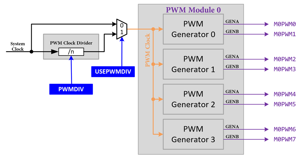
Figure 13.1: PWM Module Block Diagram
Inside the PWM Module — Figure 13.1
Figure 13.1 shows the block diagram of one complete PWM module. Read it left to right as a signal flow: a clock comes in, four generators build the raw waveforms, and an output stage decides what finally reaches the pins. The blocks are:
| Block in Figure 13.1 | What it does |
|---|---|
| PWM Clock | Feeds the counting clock to all four generators. The source is either the system clock directly or the system clock passed through the PWM clock divider (see the next section). |
| Control & Status block | The module-level "master." It synchronizes update timing so that several generators can reload their LOAD/CMP values together, gathers each generator's interrupt and ADC-trigger requests, and manages module-wide fault handling. |
| PWM Generator 0–3 (four identical blocks) |
Each generator is where a waveform is actually built. Inside each one: a 16-bit timer, two comparators (CMPA / CMPB), the signal generator (action logic), and a dead-band generator. Each block outputs two internal signals, pwmA and pwmB. |
| Output Control block | Sits between the eight internal signals and the device pins. It enables or disables each output, optionally inverts its polarity, and forces outputs to a programmed level when a fault occurs. Only signals that pass this stage reach a pin. |
| Fault condition inputs | External fault signals (and comparator/ADC-based conditions) that the module can react to immediately in hardware, independently of software. |
| Interrupt & Trigger generation | Turns generator events (zero, load, compare match) into interrupts to the CPU and trigger pulses to the ADC, so sampling can be time-aligned to the PWM waveform. |
How a generator maps to output numbers. The four generators are wired to the eight outputs in fixed pairs. This mapping is worth memorizing early, because the output name (e.g., M0PWM4) encodes exactly which generator and which of its two signals is meant:
| Generator | pwmA output | pwmB output |
|---|---|---|
| Generator 0 | PWM0 | PWM1 |
| Generator 1 | PWM2 | PWM3 |
| Generator 2 | PWM4 | PWM5 |
| Generator 3 | PWM6 | PWM7 |
We will decode a full output name, such as M0PWM4 — module, generator, signal A/B, and output number — in a later section on the PCTL table.
The big picture. Everything after this section — the clock divider, the timer, the compare registers, and the signal generator — lives inside one of the four generator blocks of Figure 13.1. Keep this diagram in mind as the map; the rest of the lesson zooms in on one generator and examines each part in turn.
13.2 PWM Clock Configuration
PWM Clock Configuration
Figure 13.1: PWM Module Block Diagram
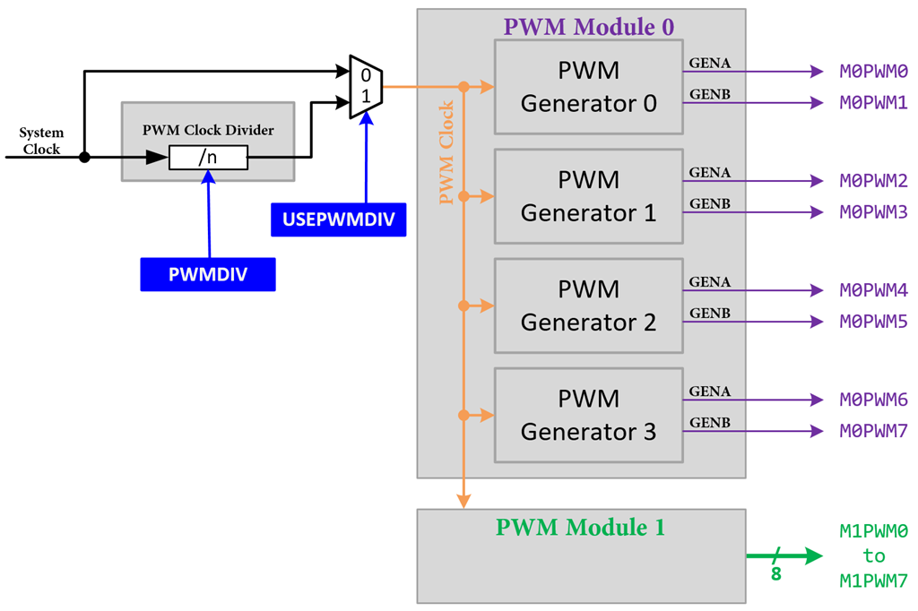
The leftmost block in Figure 13.1 is the PWM clock. Every generator counts on this clock, so its rate sets the time base for all eight PWM outputs. The module gives you two source choices:
- The system clock directly, or
- The system clock passed through a PWM clock divider (a pre-divided version of the system clock).
The choice is made with two fields: the USEPWMDIV bit turns the divider on or off, and the PWMDIV field selects the divisor. On the two boards, these fields live in different registers:
- EK-TM4C123GXL: fields are in the Run-Mode Clock Configuration register, RCC.
- EK-TM4C1294XL: fields are in the PWM Clock Configuration register, PWMCC.
The field names and their meaning are identical; only the host register differs. This is the one place a program written for one board will not compile for the other.
The divider is a simple power-of-two prescaler:
| PWMDIV | Divisor | PWM clock (from an 80 MHz system clock) |
|---|---|---|
| 0x0 | ÷ 2 | 40 MHz |
| 0x1 | ÷ 4 | 20 MHz |
| 0x2 | ÷ 8 | 10 MHz |
| 0x3 | ÷ 16 | 5 MHz |
| 0x4 | ÷ 32 | 2.5 MHz |
| 0x5 – 0x7 | ÷ 64 | 1.25 MHz |
The divider only takes effect when USEPWMDIV is set to 1. If it is 0, the PWM clock equals the system clock, and the PWMDIV value is ignored.
Why Do We Need a PWM Clock Divider?
The answer comes entirely from one hardware limit: the PWM timer is only 16 bits wide. That means the largest LOAD value it can hold is 65,535, and the PWM frequency in Count-Down mode is:
fPWM = fPWMCLK ÷ (LOAD + 1)
Since LOAD cannot exceed 65,535, the lowest frequency you can reach is fixed by the PWM clock:
fPWM,min = fPWMCLK ÷ 65,536
Run the numbers with no divider, and the problem is obvious:
| Board | System clock | Lowest fPWM with no divider | Lowest fPWM with ÷64 |
|---|---|---|---|
| TM4C123G | 80 MHz | ≈ 1221 Hz | ≈ 19 Hz |
| TM4C1294 | 120 MHz | ≈ 1831 Hz | ≈ 29 Hz |
Without the divider, a TM4C123G simply cannot produce anything below about 1.2 kHz — no matter what LOAD value you choose. Yet many everyday jobs need far lower frequencies: a hobby servo wants 50 Hz, LED dimming, and simple motor drive often sit in the tens to low hundreds of Hz. The divider is what makes those reachable — but you must choose the divisor carefully, not just reach for the biggest one.
Do not default to ÷64. The goal is always to make LOAD as large as possible without exceeding 65,535, because LOAD is your duty-cycle resolution. Reaching for the largest divisor "just to be safe" quietly halves or quarters your resolution. Pick the smallest divisor whose LOAD still fits.
The method — maximize LOAD. For a target frequency fPWM, walk the divisors from smallest to largest and compute LOAD for each, then stop at the first (largest-clock) one that fits in 16 bits:
LOAD = fPWMCLK ÷ fPWM − 1 (must be ≤ 65,535)
Worked example — 50 Hz servo on TM4C123G (system clock = 80 MHz). Test divisors from the smallest up and keep the largest LOAD that fits:
- No divider (80 MHz): LOAD = 80,000,000 ÷ 50 − 1 = 1,599,999 → overflow.
- ÷16 (5 MHz): LOAD = 5,000,000 ÷ 50 − 1 = 99,999 → still overflow.
- ÷32 (2.5 MHz): LOAD = 2,500,000 ÷ 50 − 1 = 49,999 → fits, and it is the largest LOAD that fits. ✔ Use this.
- ÷64 (1.25 MHz): LOAD = 24,999 → also fits, but throws away half the resolution.
So the correct choice is ÷32 with LOAD = 49,999 — not ÷64.
The system clock is a second lever. The system clock is reconfigurable — up to 80 MHz on the TM4C123G and 120 MHz on the TM4C1294. Since the PWM clock is derived from it, changing the system clock also shifts every LOAD value. This matters at the extremes: for a very low target frequency, even ÷64 can overflow (e.g., 5 Hz on 80 MHz gives LOAD = 249,999 even at ÷64), and the only remaining fix is to lower the system clock. Conversely, running the system clock at its maximum generally gives you the finest resolution at higher PWM frequencies. In practice: set the system clock for the CPU's needs first, then pick the divisor that maximizes LOAD for your PWM frequency.
Choosing the Clock Source in Setup_PWM()
The PWM clock is not automatically selected for you — selecting it is an explicit step in Setup_PWM(). For the dedicated PWM module, there are exactly two source options, and USEPWMDIV is the selector:
- USEPWMDIV = 0 → The undivided system clock feeds the PWM module.
- USEPWMDIV = 1 → The divided system clock (rate set by PWMDIV) feeds the PWM module.
Note that the "system clock" itself is whatever you programmed during clock initialization — it can be derived from the internal oscillator (PIOSC), the external main oscillator (MOSC), or the PLL. That choice is made when the system clock is set up, not here; Setup_PWM() simply decides whether to use the system clock directly or via the divider.
Which do we prefer in general? Start with the undivided system clock (USEPWMDIV = 0). The faster the PWM clock, the more counts fit in one period, so you get the finest duty-cycle resolution and the widest reach toward high frequencies. Turn the divider on only when your target frequency is so low that the required LOAD would overflow the 16-bit counter — the classic case being a 50 Hz servo, where a divisor is unavoidable.
A note on "ALTCLK". On the TM4C1294, the datasheet describes a global alternate-clock resource (ALTCLK = PIOSC, RTCOSC, or LFIOSC, selected in ALTCLKCFG). That resource serves the general-purpose timers, SSI, and UART — not the dedicated PWM module. The PWM module in this lesson always runs from the system clock (undivided or divided). If you see "PWM" mentioned alongside ALTCLK in the datasheet's clock overview, it refers to a PWM waveform produced by a general-purpose timer, which is a different mechanism from the PWM module covered here.
13.3 PWM Timer
PWM Timer
At the heart of every PWM generator is a single 16-bit counter — the PWM timer. It is clocked by the PWM clock selected in the previous section and counts continuously once the generator is enabled, with no CPU involvement. Two registers and one control bit define its behavior:
- PWMnLOAD holds the LOAD value—the top of the count that sets the PWM period.
- The MODE bit in PWMnCTL selects the counting mode: 0 = Count-Down, 1 = Count-Up/Down.
Because both outputs of a generator (pwmA and pwmB) share this one timer, they always run at the same frequency.
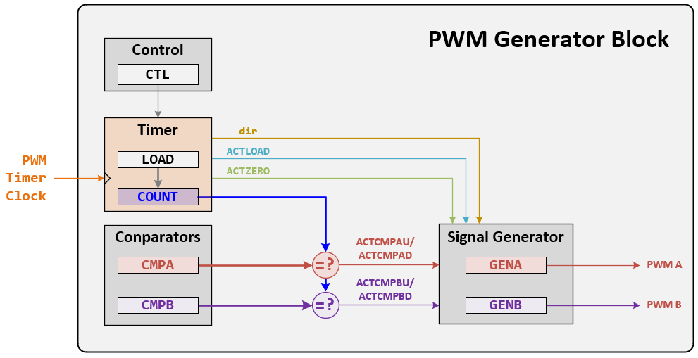
Figure 13.2: PWM Generator Block Diagram
The Three Timer Signals: dir, ACTZERO, ACTLOAD
The timer does not directly drive any pin. Instead, it emits three internal signals that the comparators and the signal generator consume. These are the signals drawn in Figure 13.3(a) and Figure 13.3(b):
| Signal | What it is |
|---|---|
| dir | The direction signal. It marks whether the counter is currently counting up or down, and is used to qualify the comparator matches (up-match vs. down-match). |
| ACTZERO | A single-clock-cycle-width High pulse is emitted the instant the counter reaches 0. |
| ACTLOAD | A single-clock-cycle-width High pulse is emitted the instant the counter reaches the LOAD value. |
The signal generator takes these pulses — together with the comparator pulses ACTCMPAD, ACTCMPAU, ACTCMPBD, ACTCMPBU, all qualified by dir — and turns them into the two output waveforms. (How that happens is the subject of the Signal Generator section.)
One rule to remember: a comparator match is ignored whenever it coincides with an ACTZERO or ACTLOAD event — the zero and load actions win. And if a CMPA match and a CMPB match land on the same tick, pwmA follows only CMPA, and pwmB follows only CMPB.
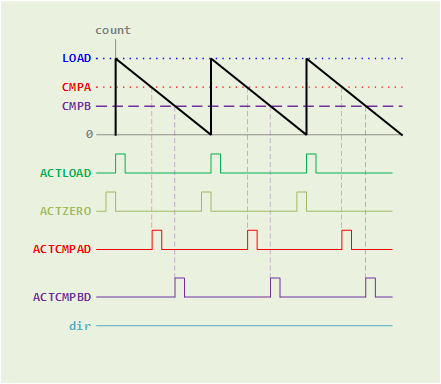
Figure 13.3 (a): PWM Count-Down Mode
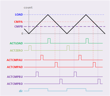
Figure 13.3 (b): PWM Count-UP/Down Mode
Count-Down Mode
Count-Down Mode
In Count-Down mode, the counter starts at LOAD, decrements once per PWM clock down to 0, then reloads LOAD and repeats:
LOAD → LOAD−1 → … → 1 → 0 → (reload) LOAD → …
Follow the three signals through one period — this is exactly Figure 13.3(a):
- dir stays Low the whole time — there is only one counting direction, so the comparators produce only "down" matches (ACTCMPAD / ACTCMPBD).
- ACTZERO fires as the counter hits 0.
- ACTLOAD fires on the very next clock, when the counter reloads LOAD. So in Count-Down mode, the zero pulse is immediately followed by the load pulse — the two sit back-to-back at the bottom of every period.
The counter visits LOAD+1 distinct values (LOAD down through 0), so one full period takes LOAD + 1 PWM clocks:
fPWM = fPWMCLK ÷ (LOAD + 1)
This mode generates left- and right-aligned PWM signals.
Why LOAD + 1, and why LOAD = period − 1? A counter that runs from LOAD down to 0 passes through LOAD + 1 counts, not LOAD. That is why, when you want a period of N clocks, you program LOAD = N − 1. Forgetting the "−1" is the classic off-by-one error that causes a measured frequency to drift slightly from the target.
Count-Up/Down Mode
Count-Up/Down Mode
In Count-Up/Down mode, the counter ramps up from 0 to LOAD, then back down to 0, and repeats — a triangle instead of a sawtooth:
0 → 1 → … → LOAD → LOAD−1 → … → 1 → 0 → 1 → …
Now trace the three signals — this is Figure 13.3(b):
- dir now alternates: it takes one value while the counter climbs and the other while it descends, flipping once each half-period. This is the crucial difference from Count-Down mode.
- Because the counter passes each compare value twice per period — once going up, once going down — dir determines whether it is an up-match (ACTCMPAU) or a down-match (ACTCMPAD).
- ACTZERO fires at the bottom of the triangle (counter = 0); ACTLOAD fires at the top (counter = LOAD). Unlike Count-Down mode, these two pulses now sit at opposite ends of the period.
One full up-and-down trip takes 2 × LOAD PWM clocks, so the frequency is half of what the same LOAD would give in Count-Down mode:
fPWM = fPWMCLK ÷ (2 × LOAD)
This mode generates center-aligned PWM signals.
The whole point of dir. A single compare value can only ever equal the counter at one number, but in Count-Up/Down mode, the counter reaches that number twice per period. The dir signal is what lets the hardware treat those two crossings as two separate, independently programmable events. That is precisely what makes a symmetric, center-aligned pulse possible.
Summary: The Timer Signals in Both Modes
| Signal | Count-Down mode | Count-Up/Down mode |
|---|---|---|
| dir | Always Low | Alternates every half-period (up vs. down) |
| ACTZERO | High pulse at counter = 0, immediately followed by ACTLOAD | High pulse at the bottom of the triangle (counter = 0) |
| ACTLOAD | High pulse at the counter = LOAD, right after the reload | High pulse at the top of the triangle (counter = LOAD) |
| Compare matches | Down only: ACTCMPAD, ACTCMPBD | Both directions: ACTCMPAU/AD, ACTCMPBU/BD |
| Period (clocks) | LOAD + 1 | 2 × LOAD |
| Used for | Left- / Right-aligned PWM | Center-aligned PWM |
13.4 PWM Compare Registers
PWM Compare Registers
Each PWM generator has two 16-bit compare registers, PWMnCMPA and PWMnCMPB. On every PWM clock, the timer's current count is compared against both values. The instant the counter equals a compare value, that comparator emits a match pulse — the same ACTCMPAD / ACTCMPAU / ACTCMPBD / ACTCMPBU pulses the signal generator uses, qualified by dir.
Where the LOAD value sits at the top of the count and never moves during operation, a compare value marks a point inside the count — the moment at which the output is told to switch. Moving that point is how you set the duty cycle.
Notation. The two compare registers behave identically — the only difference is which output they drive. So in the calculations that follow we write a single symbol, CMP, to mean "CMPA or CMPB." You substitute the concrete register (PWMnCMPA or PWMnCMPB) only when you write the setup code, discussed later.
Figure 13.2: PWM Generator Block Diagram
How the Compare Value Sets the Duty Cycle
This gives you two cleanly separated knobs:
LOAD sets the frequency; CMP sets the duty cycle. Change CMP and only the duty moves — the period, and therefore the frequency, is untouched. That independence is exactly what LED dimming and motor-speed control rely on: keep the frequency fixed, sweep the compare value.
What a given compare value does to the duty depends on which actions the signal generator has assigned to the match — that is, on the alignment:
| Alignment | High time (counts) | Duty cycle D | As CMP increases… |
|---|---|---|---|
| Left-aligned | LOAD − CMP | (LOAD − CMP) / (LOAD + 1) | duty decreases |
| Right-aligned | CMP | CMP / (LOAD + 1) | duty increases |
| Center-aligned | 2 × (LOAD − CMP) | (LOAD − CMP) / LOAD | duty decreases |
So a compare value on its own does not "mean" a fixed duty — the same CMP can give a large or a small duty depending on whether the generator is configured left- or right-aligned. Always read the compare value together with the action configuration.
The Valid Range of a Compare Value
A compare value is useful only if the counter can actually reach it and the resulting match is not discarded. From the timer rules in the previous section, that pins down the range:
A compare value is honored only if the counter can reach it during normal counting, and the resulting match is not overridden by a timer event. The datasheet pins down two boundary cases:
- CMP > LOAD → the counter never climbs above LOAD, so the comparator never outputs a High pulse (per the datasheet: a comparator value greater than the load value produces no match).
- CMP = LOAD → the counter only ever equals LOAD at the single instant it reloads — which is exactly when ACTLOAD fires. Because a match that coincides with the load (or zero) event is ignored, the load action overrides it, and you get no usable switching edge.
The value 0, by contrast, is perfectly legal: it is a count that the timer genuinely passes through, so writing CMP = 0 gives well-defined behavior (the extreme duty is realized through the level set at ACTLOAD, not through a compare edge).
Valid range: 0 ≤ CMP ≤ LOAD − 1. The compare value can be zero, but it must never be greater than or equal to LOAD — so the largest possible compare value is LOAD − 1. Writing CMP = LOAD (or higher) does not give you "almost 100%"; the match is suppressed, and the output silently sits at a constant level instead.
To get an exact 0% or 100% duty cycle, do not rely on an out-of-range compare value. Instead, force the output to a constant level (for example, with the output-control or the generator's "always drive" actions), or simply disable that PWM output.
Computing a Compare Value from a Target Duty
In practice, you decide the duty first and solve for CMP. Rearranging the table above:
| Alignment | CMP for a duty of D |
|---|---|
| Left-aligned | CMP = LOAD − D × (LOAD + 1) |
| Right-aligned | CMP = D × (LOAD + 1) |
| Center-aligned | CMP = LOAD × (1 − D) |
Worked example — 25% duty, LOAD = 999 (a 1000-count period).
- Left-aligned: CMP = 999 − 0.25 × 1000 = 749. High time = LOAD − CMP = 999 − 749 = 250 counts = 25%. ✔
- Right-aligned: CMP = 0.25 × 1000 = 250. High time = CMP = 250 counts = 25%. ✔
Both land safely inside 0 … LOAD − 1 (that is, 0 … 998), so both are valid.
Two Independent Compares: CMPA and CMPB
Because CMPA and CMPB are separate registers driving separate outputs, one generator can output two different duty cycles on pwmA and pwmB, while, because they share the timer, both stay locked to the same frequency. This allows a single generator to produce either two unrelated PWM signals or a complementary pair for driving an H-bridge.
13.5 PWM Signal Generator
PWM Signal Generator
The signal generator is where everything from the previous sections comes together. It consumes the timer's dir, ACTZERO, and ACTLOAD pulses together with the comparator's ACTCMPAD / ACTCMPAU / ACTCMPBD / ACTCMPBU pulses, and from them it builds the two output waveforms. It is programmed through two registers of identical layout: PWMnGENA builds pwmA, and PWMnGENB builds pwmB.
The timer and comparator decide when; the signal generator decides what to do. A comparator only reports the instant its value is matched — it has no opinion about whether the output should go high or low. That decision is entirely programmable, and it is exactly what makes one set of hardware capable of producing left-, right-, or center-aligned PWM.
Action Fields and Action Codes
Each generator register is a stack of six 2-bit fields, one per event. Each field says what should happen to the output the moment that event fires:
| Bit field | Name | Fires when… |
|---|---|---|
| [1:0] | ACTZERO | counter = 0 |
| [3:2] | ACTLOAD | counter = LOAD |
| [5:4] | ACTCMPAU | (pwmA) counter = CMP, counting up |
| [7:6] | ACTCMPAD | (pwmA) counter = CMP, counting down |
| [9:8] | ACTCMPBU | (pwmB) counter = CMP, counting up |
| [11:10] | ACTCMPBD | (pwmB) counter = CMP, counting down |
The value placed in any field is a 2-bit action code:
| Code | Action on the output |
|---|---|
| 0x0 | Do nothing |
| 0x1 | Invert the output |
| 0x2 | Drive the output Low |
| 0x3 | Drive the output High |
To build pwmA, you normally program only the ACTLOAD and the ACTCMPA fields, leaving everything else at 0x0. Recall the two rules from earlier: the counting mode comes from the MODE bit in PWMnCTL, and a match that coincides with a zero or load event is ignored.
Derive the value with the MyDefines.h macros. Instead of a bare hex constant, build the generator value from named actions and event positions — the code then reads exactly like the recipe. For example, "drive High on LOAD, drive Low on CMP-down" becomes (_PWM_GEN_ACT_PWM_LOW << _PWM_GEN_ACTCMPAD_BIT) | (_PWM_GEN_ACT_PWM_HIGH << _PWM_GEN_ACTLOAD_BIT), which evaluates to (0x2 << 6) | (0x3 << 2) = 0x8C. Read the number off the datasheet only to check your work.
Generating the Three Alignments
Left-aligned (Count-Down mode). Referring to the down-count sawtooth of Figure 13.3(a): drive High at the start of the period and Low at the compare point, so the pulse hugs the left edge.
- ACTLOAD [3:2] → Drive High, ACTCMPAD [7:6] → Drive Low
- GENA = (_PWM_GEN_ACT_PWM_LOW << _PWM_GEN_ACTCMPAD_BIT) | (_PWM_GEN_ACT_PWM_HIGH << _PWM_GEN_ACTLOAD_BIT) = 0x8C
Right-aligned (Count-Down mode). Same sawtooth, actions swapped: drive Low at the start and High at the compare point, so the pulse hugs the right edge.
- ACTLOAD [3:2] → Drive Low, ACTCMPAD [7:6] → Drive High
- GENA = (_PWM_GEN_ACT_PWM_HIGH << _PWM_GEN_ACTCMPAD_BIT) | (_PWM_GEN_ACT_PWM_LOW << _PWM_GEN_ACTLOAD_BIT) = 0xC8
Center-aligned (Count-Up/Down mode). Referring to the triangle of Figure 13.3(b): the counter crosses the compare value twice, so use both crossings to place a High pulse symmetrically around the peak.
- ACTCMPAU [5:4] → Drive High, ACTCMPAD [7:6] → Drive Low (ACTLOAD and ACTZERO stay at "do nothing")
- GENA = (_PWM_GEN_ACT_PWM_LOW << _PWM_GEN_ACTCMPAD_BIT) | (_PWM_GEN_ACT_PWM_HIGH << _PWM_GEN_ACTCMPAU_BIT) = 0xB0
| Alignment | Counter mode | Actions used | GENA |
|---|---|---|---|
| Left-aligned | Count-Down | LOAD→High, CMPAD→Low | 0x8C |
| Right-aligned | Count-Down | LOAD→Low, CMPAD→High | 0xC8 |
| Center-aligned | Count-Up/Down | CMPAU→High, CMPAD→Low | 0xB0 |
Ready-made macros. MyDefines.h already bundles the two Count-Down recipes so you can drop them straight into PWMnGENA / PWMnGENB:
- Left-aligned: _PWM_GENA_LEFT_ALIG_CMPAD (pwmA), _PWM_GENB_LEFT_ALIG_CMPBD (pwmB)
- Right-aligned: _PWM_GENA_RIGHT_ALIG_CMPAD (pwmA), _PWM_GENB_RIGHT_ALIG_CMPBD (pwmB)
There is no bundled center-aligned macro — build it from the fields as shown above, since it needs the Count-Up/Down actions.
pwmB is built the same way. To produce the second output, program PWMnGENB with the same recipes, using the ACTCMPBD / ACTCMPBU fields and the CMPB compare value. Because both outputs share a single timer, they maintain the same frequency while carrying whatever duty each compares to the set values.
13.6 Reading the PWM I/O Table: Decoding MnPWMx and Sizing LOAD / CMP
Reading the PWM I/O Table: Decoding MnPWMx and Sizing LOAD / CMP
Before you can write Setup_PWM() and Setup_GPIO(), you must answer five questions about the signal you want: which module, which generator, pwmA or pwmB, which output number, and which pin (with its PMC value). Every one of these is encoded in a PWM signal name, such as M0PWM4, and read off the PWM I/O table. This section shows how.
Finding a PWM Pin in the PCTL Table
A PWM signal can only leave the chip on a pin whose Port Control (PCTL) register is set to the correct alternate function. The PWM I/O table below is a filtered view of the full PCTL table (see Lesson 10), showing only the PWM entries. To use it:
- Find the row for the PWM signal you want (for example, M0PWM3).
- Read the GPIO Port.Pin column to get the pin, and the number in parentheses, which is the PMC (port mux code) for that function.
- Write it as GPIOx->PCTL = PMC << _PCTL_PINn; — for example GPIOB->PCTL = 0x4 << _PCTL_PIN5; for PB5.
- If a row lists two pins (such as M0PWM6 on PC4 or PD0), either pin works — pick whichever is free on your board.
The PMC is not a fixed "PWM = one number". The same PWM function appears under different PMC values on different pins and different chips. On the TM4C123G most PWM pins use PMC 0x4 (Module 0) or 0x5 (Module 1); on the TM4C1294 they use 0x6. Never copy a PMC from one board to another — always read it from that board's own table.
Decoding MnPWMx
The signal name splits into Mn (the module) and PWMx (the output number). From those two numbers, you can recover everything else:
| What you need | How to get it from MnPWMx | Used in code as |
|---|---|---|
| Module m | the digit after M | PWMm->, and RCGCPWM bit |
| Output number x | the digit after PWM | PWMm->ENABLE = _PWMx |
| Generator g | g = ⌊x ÷ 2⌋ | _g_CTL / _g_LOAD / _g_GENx / _g_CMPx |
| pwmA or pwmB | x even → pwmA, x odd → pwmB | A → GENA/CMPA, B → GENB/CMPB |
Worked decode — M0PWM4.
- Module = 0 → use PWM0->
- Output number = 4 → PWM0->ENABLE = _PWM4
- Generator = ⌊4 ÷ 2⌋ = 2 → PWM0->_2_CTL, _2_LOAD, …
- 4 is even → pwmA → use PWM0->_2_GENA and PWM0->_2_CMPA
TM4C123G vs. TM4C1294 — same rule, different details.
- Module count. The TM4C123G has two modules (M0 and M1), so both M0PWMx and M1PWMx exist. The TM4C1294 has only M0.
- Pin and PMC differ per board. The same name maps to different hardware: M0PWM1 is PB7 at PMC 0x4 on the TM4C123G, but PF1 at PMC 0x6 on the TM4C1294.
- GPIO bus. On the TM4C1294, PWM pins are reached through the AHB aperture, so the code uses GPIOx_AHB-> (e.g., GPIOF_AHB->PCTL), whereas the TM4C123G uses the APB alias GPIOx->.
Three signals from the example programs, decoded and cross-checked against the table:
| Signal | Board | Pin (PMC) | m | g = ⌊x/2⌋ | A/B | Registers |
|---|---|---|---|---|---|---|
| M0PWM3 | 123G | PB5 (0x4) | 0 | 1 | B (odd) | PWM0->_1_GENB / _1_CMPB |
| M1PWM7 | 123G | PF3 (0x5) | 1 | 3 | B (odd) | PWM1->_3_GENB / _3_CMPB |
| M0PWM1 | 1294 | PF1 (0x6) | 0 | 0 | B (odd) | PWM0->_0_GENB / _0_CMPB |
Calculating the LOAD Value
The PWM counter is clocked by the PWM clock, which is the system clock, optionally divided by the PWM divider:
fPWMCLK = SysClk ÷ PWMDIV
Here, PWMDIV is the divisor (2, 4, 8, …, 64). A value of PWMDIV = 1 means the divider is not used (USEPWMDIV = 0), so the PWM clock equals the system clock. With the PWM clock known, the LOAD value depends on the counting mode:
| Alignment | Counter mode | LOAD |
|---|---|---|
| Left- / Right-aligned | Count-Down | LOAD = (fPWMCLK ÷ fPWM) − 1 |
| Center-aligned | Count-Up/Down | LOAD = fPWMCLK ÷ (2 × fPWM) |
Because the counter is 16-bit, LOAD must fit in 65,535. Choose the smallest PWMDIV that keeps LOAD within range, so LOAD lands as close to 65,535 as possible — that maximizes duty-cycle resolution.
The "−1" and when you may drop it. The exact Count-Down formula subtracts 1 because a counter running from LOAD down to 0 spans LOAD + 1 counts. The relative error of ignoring it is about 1 ÷ (LOAD + 1). At LOAD = 39,999, using a round 40,000 shifts a 1 kHz output by only 0.0025% (to 1000.025 Hz) — undetectable. So when LOAD is large (roughly ≥ 1000), you may use the round integer and drop the −1. When LOAD is small (a high PWM frequency — say LOAD = 99), ±1 is a full 1% error, so keep the −1.
Calculating the Initial CMP Value (Duty = 0)
For initialization, we usually set all outputs to 0% duty and change them later at runtime. The comparison value for a duty of D depends on the alignment, and setting D = 0 exposes an important subtlety:
| Alignment | CMP for duty D | CMP at D = 0 | Initial value to use |
|---|---|---|---|
| Left-aligned | CMP = LOAD − D × (LOAD + 1) | CMP = LOAD (out of range) | CMP = LOAD − 1 |
| Right-aligned | CMP = D × (LOAD + 1) | CMP = 0 (valid) | CMP = 0 |
| Center-aligned | CMP = LOAD × (1 − D) | CMP = LOAD (out of range) | CMP = LOAD − 1 |
Keep CMP in range: 0 ≤ CMP < LOAD (maximum LOAD − 1). Right-aligned gives CMP = 0 for 0% duty, which is fine. But left- and center-aligned both compute CMP = LOAD for 0% duty, and CMP = LOAD is not allowed — the match coincides with the load event and is ignored. Whenever the calculation yields CMP = LOAD, use CMP = LOAD − 1 instead. That gives the narrowest legal pulse (one count wide), effectively 0%. For a truly exact 0% or 100%, drive the output to a constant level or disable it instead.
Worked Examples
Example 1 — Right-aligned, 1 kHz, TM4C123G. SysClk = 80 MHz, PWMDIV = 2 → fPWMCLK = 80 ÷ 2 = 40 MHz.
- LOAD = (40,000,000 ÷ 1000) − 1 = 39,999. LOAD is large, so the round value 40,000 is also fine (0.0025% off).
- Initial CMP (right-aligned, 0% duty) = 0.
Example 2 — Left-aligned, 50 Hz servo, TM4C1294. SysClk = 40 MHz, PWMDIV = 16 → fPWMCLK = 40 ÷ 16 = 2.5 MHz.
- LOAD = (2,500,000 ÷ 50) − 1 = 49,999 (round 50,000 also fine).
- A servo wants a 1–2 ms pulse inside the 20 ms (50 Hz) period. For a 1 ms pulse, duty D = 1 ÷ 20 = 0.05, so CMP = LOAD × (1 − 0.05) = 50,000 × 0.95 = 47,500.
- For a 2 ms pulse, D = 2 ÷ 20 = 0.10, so CMP = LOAD × (1 − 0.10) = 50,000 × 0.90 = 45,000.
Example 3 — Center-aligned, 20 kHz, 25% duty, TM4C123G. SysClk = 80 MHz. First, pick the divisor that keeps LOAD closest to 65,535:
- PWMDIV = 1 (no divider, 80 MHz): LOAD = 80,000,000 ÷ (2 × 20,000) = 2,000 → valid but small.
- To push LOAD higher, we would need a faster clock; 80 MHz is the max, so LOAD = 2,000 at PWMDIV = 1 is the best resolution available here. (A divider would only make LOAD smaller.)
- Initial CMP at 25% duty = LOAD × (1 − 0.25) = 2,000 × 0.75 = 1,500. For 0% initialization, it would be CMP = LOAD = 2,000 → use 1,999 instead.
The full chain. Every example follows the same path: SysClk → (÷ PWMDIV) → fPWMCLK → LOAD → CMP. Decode the name to know which registers to write these values into, and you are ready to fill in Setup_PWM().
13.7 Implementing Setup_PWM(): From MnPWMx to Registers
Implementing Setup_PWM(): From MnPWMx to Registers
Everything so far — decoding MnPWMx, choosing the divider, computing LOAD and CMP, and picking the generator actions — now lands in one function. Setup_PWM() follows the same six steps every time; only the numbers and the decoded register names change.
Recall the register naming from the decode step: m is the module (PWMm->), g is the generator (_g_, from ⌊x÷2⌋), and A/B follows the parity of the output number.
The Six Steps
| Step | What it does | Key register/macro |
|---|---|---|
| 1. Clock the module | Turn on the PWM module clock, then wait until it is ready. | RCGCPWM, PRPWM, _PWM_MODULE0/1 |
| 2. Set the divider | Select the PWM clock source (undivided or divided) and the divisor. This register differs per board. | 123G: SYSCTL->RCC 1294: PWMm->CC |
| 3. Disable + pick mode | Write 0 to the generator control register while you configure it. A cleared register is already in Count-Down mode. | PWMm->_g_CTL = 0x00 |
| 4. LOAD / CMP / GEN | Program the period (LOAD), the initial duty (CMP), and the alignment actions (GEN). | _g_LOAD, _g_CMPx, _g_GENx |
| 5. Enable the generator | Start the counter and confirm the mode. | _g_CTL |= _PWM_BLOCK_ENABLE | _PWM_COUNT_DOWN_MODE |
| 6. Enable the output | Route the internal signal to the module's output pin. | PWMm->ENABLE = _PWMx |
Step 2 is the one place where the two boards genuinely differ. On the TM4C123G, the divider lives in the System Control register SYSCTL->RCC. On the TM4C1294, it lives in the PWM module's own clock-configuration register, PWMm->CC (e.g., PWM0->CC) — not SYSCTL->CC. Everything else in the two functions is identical.
Example 1 — TM4C123G: Two PWMs (M0PWM3 + M1PWM7)
Example 1 — TM4C123G: Two PWMs (M0PWM3 + M1PWM7)
Two right-aligned outputs at 1 kHz: M0PWM3 on PB5 (a motor) and M1PWM7 on PF3 (an LED). Decoding first:
- M0PWM3 → module 0, generator ⌊3÷2⌋ = 1, odd → pwmB → PWM0->_1_GENB / _1_CMPB
- M1PWM7 → module 1, generator ⌊7÷2⌋ = 3, odd → pwmB → PWM1->_3_GENB / _3_CMPB
Clock math: SysClk = 80 MHz, PWMDIV = 2 → fPWMCLK = 40 MHz. For 1 kHz, LOAD = 40,000,000 ÷ 1000 − 1 = 39,999; since LOAD is large, the round 40,000 is used, and the −1 is negligible. Initial duty is 0%, and right-aligned takes CMP = 0.
void Setup_PWM(void)
{   // Two PWMs: M0PWM3 (PB5, motor) and M1PWM7 (PF3, LED), right-aligned, 1 kHz

    // 1. Enable clock for PWM Modules 0 and 1
    SYSCTL->RCGCPWM |= (_PWM_MODULE0 | _PWM_MODULE1);
    while((SYSCTL->PRPWM & (_PWM_MODULE0 | _PWM_MODULE1)) != (_PWM_MODULE0 | _PWM_MODULE1)){};

    // 2. Enable and set the PWM clock divider  (123G: SYSCTL->RCC)
    SYSCTL->RCC |=  (_PWM_123G_USEPWMDIV);               // RCC[20]=1: use divider
    SYSCTL->RCC &= ~(_PWM_123G_PWMDIV_MASK);            // RCC[19:17]=000
    SYSCTL->RCC |=  (_PWMDIV_2 << _PWM_123G_PWMDIV_BIT); // RCC[19:17]=/2 -> 40 MHz

    // 3. Disable the generators (0x00 is also Count-Down mode)
    PWM0->_1_CTL = 0x00;
    PWM1->_3_CTL = 0x00;

    // 4. LOAD / CMP / GEN
    PWM0->_1_LOAD = 40000;                               // 1 kHz
    PWM0->_1_CMPB = 0;                                   // 0% duty
    PWM0->_1_GENB = (_PWM_GEN_ACT_PWM_HIGH << _PWM_GEN_ACTCMPBD_BIT) |
                   (_PWM_GEN_ACT_PWM_LOW  << _PWM_GEN_ACTLOAD_BIT);   // Right-aligned

    PWM1->_3_LOAD = 40000;
    PWM1->_3_CMPB = 0;
    PWM1->_3_GENB = (_PWM_GEN_ACT_PWM_HIGH << _PWM_GEN_ACTCMPBD_BIT) |
                   (_PWM_GEN_ACT_PWM_LOW  << _PWM_GEN_ACTLOAD_BIT);   // Right-aligned

    // 5. Enable the generators
    PWM0->_1_CTL |= _PWM_BLOCK_ENABLE | _PWM_COUNT_DOWN_MODE;
    PWM1->_3_CTL |= _PWM_BLOCK_ENABLE | _PWM_COUNT_DOWN_MODE;

    // 6. Enable the outputs
    PWM0->ENABLE  = _PWM3;
    PWM1->ENABLE  = _PWM7;
}
To change the duty at run time, write a new value to PWM0->_1_CMPB / PWM1->_3_CMPB anywhere in the range 0 … LOAD − 1.
Example 2 — TM4C1294: Servo (M0PWM1)
Example 2 — TM4C1294: Servo (M0PWM1)
One left-aligned 50 Hz output on M0PWM1 (PF1) to drive a hobby servo. Decoding: module 0, generator ⌊1÷2⌋ = 0, odd → pwmB → PWM0->_0_GENB / _0_CMPB.
Clock math: SysClk = 40 MHz, PWMDIV = 16 → fPWMCLK = 2.5 MHz. For 50 Hz, LOAD = 2,500,000 ÷ 50 = 50,000. The servo pulse maps to a duty inside the 20 ms period: a 1 ms pulse is D = 0.05 → CMP = 50,000 × (1 − 0.05) = 47,500; a 2 ms pulse is D = 0.10 → CMP = 50,000 × (1 − 0.10) = 45,000. We initialize at the 1 ms position.
void Setup_PWM(void)
{   // Servo on M0PWM1 (PF1), left-aligned, 50 Hz

    // 1. Enable clock for PWM Module 0
    SYSCTL->RCGCPWM |= (_PWM_MODULE0);
    while((SYSCTL->PRPWM & (_PWM_MODULE0)) != (_PWM_MODULE0)){};

    // 2. Enable and set the PWM clock divider  (1294: PWMm->CC, NOT SYSCTL->CC)
    PWM0->CC |=  (_PWM_1294_USEPWMDIV);                  // CC[8]=1: use divider
    PWM0->CC &= ~(_PWM_1294_PWMDIV_MASK);              // CC[2:0]=000
    PWM0->CC |=  (_PWMDIV_16 << _PWM_1294_PWMDIV_BIT);   // CC[2:0]=/16 -> 2.5 MHz

    // 3. Disable the generator (0x00 is also Count-Down mode)
    PWM0->_0_CTL = 0x00;

    // 4. LOAD / CMP / GEN
    PWM0->_0_LOAD = 50000;                               // 50 Hz
    PWM0->_0_CMPB = 47500;                               // 1 ms pulse (D = 0.05)
    PWM0->_0_GENB = (_PWM_GEN_ACT_PWM_HIGH << _PWM_GEN_ACTLOAD_BIT) |
                   (_PWM_GEN_ACT_PWM_LOW  << _PWM_GEN_ACTCMPBD_BIT);  // Left-aligned

    // 5. Enable the generator
    PWM0->_0_CTL |= _PWM_BLOCK_ENABLE | _PWM_COUNT_DOWN_MODE;

    // 6. Enable the output
    PWM0->ENABLE  = _PWM1;
}
Sweep the servo at run time by writing PWM0->_0_CMPB between the 1 ms and 2 ms values (47,500 and 45,000). Notice the servo's larger pulse means a smaller CMP here — that is the left-aligned relationship (bigger CMP → smaller duty), which is why reading CMP together with the alignment matters.
Two Things to Watch
- The divider constant is _PWM_123G_PWMDIV_BIT (with the underscore after PWM). A template that writes _PWM123G_PWMDIV_BIT will not compile.
- On the TM4C1294, step 2 uses PWMm->CC (the PWM module register). Using SYSCTL->CC is a different register and will not set the PWM divider.
The PWM engine is now running on its own. The only remaining piece is telling the GPIO pins to hand their control over to the PWM peripheral — that is Setup_GPIO(), covered next.
13.8 Implementing Setup_GPIO(): Handing the Pin to the PWM Peripheral
Implementing Setup_GPIO(): Handing the Pin to the PWM Peripheral
After Setup_PWM(), the PWM engine is already generating waveforms internally — but they cannot leave the chip until the GPIO pin is told to stop being a plain I/O and hand control to the PWM peripheral. That handover is the entire job of Setup_GPIO().
The general GPIO configuration has eight steps, but a PWM output needs only four: 1, 4, 5, and 8. The rest are shown for completeness so you can see why they are skipped.
The Eight Steps (PWM Uses Four)
| Step | Register | Needed for PWM? |
|---|---|---|
| 1. Clock the port | RCGCGPIO + wait on PRGPIO | Yes |
| 2. Unlock | LOCK / CR | Only for PD7, PF0 (123G) / PD7 (1294) |
| 3. Analog mode off | AMSEL | No (default is digital) |
| 4. Port control | PCTL = PMC << _PCTL_PINn | Yes |
| 5. Alternate function | AFSEL | Yes |
| 6. Direction | DIR | No — leave it alone (see below) |
| 7. Pull-up/down / open-drain | PUR / PDR / ODR | No (not needed for a push-pull PWM drive) |
| 8. Digital enable | DEN | Yes |
So the working core of a PWM pin setup is just three registers — PCTL, AFSEL, and DEN — after the port clock is on.
Do not set DIR on a PWM pin. Once AFSEL hands the pin to the PWM peripheral, the peripheral controls the pin's direction — it drives the output itself. Writing DIR is unnecessary and misleading; both example programs leave it untouched.
The PMC value comes from decoding, not memory. The number you shift into PCTL is the PMC you read out of the PWM I/O table for that exact pin and signal. That is why PB5 uses 0x4, PF3 uses 0x5, and PF1 (on the TM4C1294) uses 0x6 — three different pins, three different PMC values.
Example 1 — TM4C123G: PB5 (M0PWM3) and PF3 (M1PWM7)
Example 1 — TM4C123G: PB5 (M0PWM3) and PF3 (M1PWM7)
Two pins to hand over. From the PWM I/O table: PB5 → M0PWM3 at PMC 0x4; PF3 → M1PWM7 at PMC 0x5. On the TM4C123G, GPIO is reached through the APB alias GPIOx->.
void Setup_GPIO(void)
{   // PB5 -> M0PWM3 (PMC 0x4),  PF3 -> M1PWM7 (PMC 0x5)

    // 1. Enable Clock to the GPIO Modules (SYSCTL->RCGCGPIO |= (_PORTs);)
    //    Enable clock to Ports B and F, then wait
    SYSCTL->RCGCGPIO |= (_PORTB | _PORTF);
    // allow time for clock to stabilize (SYSCTL->PRGPIO & (_PORTs))
    while((SYSCTL->PRGPIO & (_PORTB | _PORTF)) != (_PORTB | _PORTF)){};

    // 2. Unlock GPIO only PD7, PF0 on TM4C123G; PD7 on TM4C1294 (GPIOx->LOCK = 0x4C4F434B; and GPIOx->CR = _PINs;)
    //    Unlock  - not needed for PB5 / PF3

    // 3. Set Analog Mode Select bits for each Port (GPIOx->AMSEL = _PINs;  0=digital, 1=analog)
    //    AMSEL   - not needed (pins are digital by default)

    // 4. Set Port Control Register for each Port (GPIOx->PCTL = PMCn << _PTCL_PINn, check the PCTL table)
    //    Port Control: select the PWM function (PMC from the PWM I/O table)
    GPIOB->PCTL = 0x4 << _PCTL_PIN5;    // PB5 = M0PWM3
    GPIOF->PCTL = 0x5 << _PCTL_PIN3;    // PF3 = M1PWM7

    // 5. Set Alternate Function Select bits for each Port (GPIOx->AFSEL = _PINs;  0=regular I/O, 1=PCTL peripheral)
    //    Alternate Function: give the pins to the peripheral
    GPIOB->AFSEL = _PIN5;
    GPIOF->AFSEL = _PIN3;

    // 6. Set Output pins for each Port (Direction of the Pins: GPIOx->DIR = _PINs;  0=input, 1=output)
    //    DIR - leave alone; the PWM peripheral drives the pin

    // 7. Set PUR bits (internal Pull-Up Resistor), PDR (Pull-Down Resistor), ODR (Open Drain) for each Port (0: disable, 1=enable)
    //    PUR / PDR / ODR - not needed

    // 8. Set Digital ENable register on all port.pins (GPIOx->DEN = _PINs; 0=disable, 1=enable)
    GPIOB->DEN = _PIN5;
    GPIOF->DEN = _PIN3;
}
Example 2 — TM4C1294: PF1 (M0PWM1)
Example 2 — TM4C1294: PF1 (M0PWM1)
One pin: PF1 → M0PWM1 at PMC 0x6. The only structural change from Example 1 is the register prefix — on the TM4C1294, PWM pins are reached through the AHB aperture, so every GPIO access uses GPIOx_AHB->.
void Setup_GPIO(void)
{   // PF1 -> M0PWM1 (PMC 0x6)

    // 1. Enable Clock to the GPIO Modules (SYSCTL->RCGCGPIO |= (_PORTs);)
    //    Enable clock to Port F, then wait
    SYSCTL->RCGCGPIO |= (_PORTF);
    // allow time for clock to stabilize (SYSCTL->PRGPIO & (_PORTs))
    while((SYSCTL->PRGPIO & (_PORTF)) != (_PORTF)){};

    // 2. Unlock GPIO only PD7, PF0 on TM4C123G; PD7 on TM4C1294 (GPIOx->LOCK = 0x4C4F434B; and GPIOx->CR = _PINs;)
    //    Unlock  - not needed for PF1

    // 3. Set Analog Mode Select bits for each Port (GPIOx->AMSEL = _PINs;  0=digital, 1=analog)
    //    AMSEL   - not needed

    // 4. Set Port Control Register for each Port (GPIOx->PCTL = PMCn << _PTCL_PINn, check the PCTL table)
    //    Port Control: select the PWM function  (note: GPIOF_AHB)
    GPIOF_AHB->PCTL = 0x6 << _PCTL_PIN1;    // PF1 = M0PWM1

    // 5. Set Alternate Function Select bits for each Port (GPIOx->AFSEL = _PINs;  0=regular I/O, 1=PCTL peripheral)
    //    Alternate Function
    GPIOF_AHB->AFSEL = _PIN1;

    // 6. Set Output pins for each Port (Direction of the Pins: GPIOx->DIR = _PINs;  0=input, 1=output)
    //    DIR - leave alone

    // 7. Set PUR bits (internal Pull-Up Resistor), PDR (Pull-Down Resistor), ODR (Open Drain) for each Port (0: disable, 1=enable)
    //    PUR / PDR / ODR - not needed

    // 8. Set Digital ENable register on all port.pins (GPIOx->DEN = _PINs; 0=disable, 1=enable)
    GPIOF_AHB->DEN = _PIN1;
}
APB vs. AHB is the usual porting trap. The TM4C123G code uses GPIOx->; the TM4C1294 code uses GPIOx_AHB->. The register layout is the same, so a program that "does nothing" on the TM4C1294 is very often just writing to the wrong aperture. Match the prefix to the board.
With both Setup_PWM() and Setup_GPIO() in place, the signal decoded from MnPWMx is now generated internally and routed out to its pin.
EK-TM4C123GXL LaunchPad
PWM Modules
The TM4C123GH6PM microcontroller contains two PWM modules; each module has four PWM generator blocks and a control block. Each PWM generator block produces two PWM signals, pwmA and pwmB. Both PWM output signals share the same PWM timer and frequency and can either be programmed with independent actions or as a single pair of complementary signals.
Each PWM generator block has the following features:
- One 16-bit counter
- Runs in Down or Up/Down mode
- PWM output frequency controlled by a 16-bit LOAD value
- Load value updates can be synchronized
- Produces output signals at zero and the LOAD value
- Two PWM comparators (CMPA, CMPB)
- Comparator value updates can be synchronized
- Produces PWM output signals on match
- PWM signal generator
- The output PWM signal is constructed based on actions taken as a result of the counter and PWM comparator output signals
- Produces two independent PWM signals (pwmA, pwmB)
PWM I/Os
| PWM Output | GPIO Port.Pins (PMCn) | PWM | ||||
| Module (m) |
Generator (g) |
Single GEN | Output | |||
| M0PWM0 | PB6 (0x4) | 0 | 0 | pwmA | PWM0 | |
| M0PWM1 | PB7 (0x4) | 0 | 0 | pwmB | PWM1 | |
| M0PWM2 | PB4 (0x4) | 0 | 1 | pwmA | PWM2 | |
| M0PWM3 | PB5 (0x4) | 0 | 1 | pwmB | PWM3 | |
| M0PWM4 | PE4 (0x4) | 0 | 2 | pwmA | PWM4 | |
| M0PWM5 | PE5 (0x4) | 0 | 2 | pwmB | PWM5 | |
| M0PWM6 | PC4 (0x4) | PD0 (0x4) | 0 | 3 | pwmA | PWM6 |
| M0PWM7 | PC5 (0x4) | PD1 (0x4) | 0 | 3 | pwmB | PWM7 |
| M1PWM0 | PD0 (0x5) | 1 | 0 | pwmA | PWM0 | |
| M1PWM1 | PD1 (0x5) | 1 | 0 | pwmB | PWM1 | |
| M1PWM2 | PA6 (0x5) | PE4 (0x5) | 1 | 1 | pwmA | PWM2 |
| M1PWM3 | PA7 (0x5) | PE5 (0x5) | 1 | 1 | pwmB | PWM3 |
| M1PWM4 | PF0 (0x5) | 1 | 2 | pwmA | PWM4 | |
| M1PWM5 | PF1 (0x5) | 1 | 2 | pwmB | PWM5 | |
| M1PWM6 | PF2 (0x5) | 1 | 3 | pwmA | PWM6 | |
| M1PWM7 | PF3 (0x5) | 1 | 3 | pwmB | PWM7 | |
Registers
Assemble
The following steps show how to initialize the PWM Generator
- Enable the clock signal for PWM module by setting its corresponding bit in the SYSCTL_RCGCPWM register, then waiting for PWM clock ready by checking the SYSCTL_PRPWM register
- Configure the Run-Mode Clock Configuration (SYSCTL_RCC) register to use the PWM divider (USEPWMDIV) and set the divider value (PWMDIV).
- Disable PWM generator by writing 0 to PWMnCTL[0] register
- Configure the PWM generator:
- Configure PWM signal by setting its corresponding bit in the PWMgpwmA and/or PWMgpwmB register
- Set the timer LOAD value to the PWMgLOAD register
- Set the pulse width value to the PWMgCMPA and/or PWMgCMPB registers
- Reset the PWM timer counter by resetting the PWM registers through the SRPWM register in the System Control Module
- Enable PWM generator by writing 1 to PWMgCTL[0] register
- Enable PWM output by setting its corresponding bit in the PWMENABLE register
After configuring the PWM, then you need to configure the GPIO pins that are connected to the PWM signal. The detailed information about GPIO configuration, please read Lesson 06: Loops.
- Enabled the clock signal to the GPIO Ports (SYSCTL_RCGCGPIO_R), then checking the ready signal (SYSCTL_PRGPIO)
- Unlock the port (GPIO_PORTn_LOCK_R). The step is needed only for PC[3:0], PD[7], and PF0 on TM4C123G. The only needing unlocking on the TM4C1294 is PD7. After unlocking the port, the appropriate bits of the GPIO Commit register (GPIO_PORTn_CR_R) need to be set.
- Disable the analog function of the pin (GPIO_PORTn_AMSEL_R)
- Configure bits in the port control register (GPIO_PORTn_PCTL_R) to select PWM function
- Configure bits in the Alternate Function Select register (GPIO_PORTn_AFSEL)
- Set the direction of the GPIO port pins (GPIO_PORTn_DIR_R)
- Program pull-up, pull-down, or open drain functionality (GPIO_PORTn_PUR_R , GPIO_PORTn_PDR_R , GPIO_PORTn_ODR_R)
- To enable GPIO pins (GPIO_PORTn_DEN_R)
C
The following steps show how to initialize PWM Generator:
- Enable the clock signal for PWM module by setting its corresponding bit in the SYSCTL->RCGCPWM register, then waiting for PWM clock ready by checking the SYSCTL->PRPWM register
- Configure the Run-Mode Clock Configuration (SYSCTL->RCC) register to use the PWM divider (USEPWMDIV) and set the divider value (PWMDIV).
- Disable PWM generator by writing 0 to PWMm->_g_CTL [0] register
- Configure the PWM generator:
- Configure PWM signal by setting its corresponding bit in the PWMm->_g_pwmA and/or PWMm->_g_pwmB register
- Set the timer LOAD value to the PWMm->_g_LOAD register
- Set the pulse width value to the PWMm->_g_CMPA and/or PWMm->_g_CMPB registers
- Reset PWM timer counter by resetting the PWM registers through the SRPWM register in the System Control Module
- Enable PWM generator by writing 1 to PWMm->_g_CTL [0] register
- Enable PWM output by setting its corresponding bit in the PWMm->ENABLE register
After configuring the PWM, then you need to configure the GPIO pins that are connected to the PWM signal. The detailed information about GPIO configuration, please read Lesson 06: Loops.
- Enabled the clock signal to the GPIO Ports (SYSCTL->RCGCGPIO |= (_PORTs);), then checking the ready signal (SYSCTL->PRGPIO)
- Unlock the port (GPIOn->LOCK). The step is needed only for PC[3:0], PD[7], and PF0 on TM4C123G. The only needing unlocking on the TM4C1294 is PD7. After unlocking the port, the appropriate bits of the GPIO Commit register (GPIOn->CR) need to be set.
- Disable the analog function of the pin (GPIOn->AMSEL)
- Configure bits in the port control register (GPIOn->PCTL) to select PWM function
- Configure bits in the Alternate Function Select register (GPIOn->AFSEL)
- Set the direction of the GPIO port pins (GPIOn->DIR)
- Program pull-up, pull-down, or open drain functionality (GPIOn->PUR, GPIOn->PDR, GPIOn->ODR)
- To enable GPIO pins (GPIOn->DEN)
The m is PWM Module number, g is the PWM Generator number, and n is the GPIO Port name.
Sample Firmware Code in Keil C
The following example code will configure the left-aligned PWM signal on PF1, which is connected with an onboard Red LED.
#include <stdio.h>
#include <stdlib.h>
#include <stdint.h>
#include <stdbool.h>

#include "TM4C123GH6PM.h"
// #include "MyDefines.h"  // Your Definition Header File

void Setup_PWM(void);
void Setup_GPIO(void);

//------------------------------------------------------------------------------
int main()
{
    Setup_PWM();
    Setup_GPIO();

    while(1){
        // Place your application code here

    }
}
//------------------------------------------------------------------------------
void Setup_PWM(void)
{
    // 1. Enable Clock for PWM Modules
    SYSCTL->RCGCPWM |= 0x02;
    while((SYSCTL->PRPWM & 0x02) != 0x02 ){};
    // 2. Enable and Setup Clock Divider for PWM Timer
    SYSCTL->RCC |= (1 << 20);       // RCC[20]=1:USEPWMDIV
    SYSCTL->RCC &= ~(0x7 << 17);    // RCC[19:17]=000 PWMDIV
    SYSCTL->RCC |= (0x4 << 17);     // RCC[19:17]=0x4 divider=/32
    // 3. Disable PWM Generator and Setup the Timer Counting Mode
    PWM1->_2_CTL = 0x00;            // Disable PWM Generator, and set to count-down mode
    // 4. Configure LOAD (Period), CMP (Duty), GEN (PWM Mode) values
    PWM1->_2_LOAD = 50000;          // Setup the period of the PWM signal
    PWM1->_2_CMPB = 50000-2250;     // Setup the initial duty cycle
    PWM1->_2_GENB = (0x02 << 10 ) | (0x03 <<2); // ACTCMPBD=ActLow ACTLOAD=ActHigh
    // 5. Enable PWM Generator
    PWM1->_2_CTL |= 0x01;
    // 6. Enable PWM Output
    PWM1->ENABLE = (1 << 5);        // Enable PWM5
}
//------------------------------------------------------------------------------
void Setup_GPIO(void)
{
    // GPIO Initialization and Configuration
    // 1. Enable Clock to the GPIO Modules (SYSCTL->RCGCGPIO |= (_PORTs);)
    SYSCTL->RCGCGPIO |= (_PORTs); |= ( );
    // allow time for clock to stabilize (SYSCTL->PRGPIO)
    while((SYSCTL->PRGPIO & (  )) != (  )){};

    // 2. Unlock GPIO only PD7, PF0 on TM4C123G; PD7, PE7 on TM4C1294 (GPIOx->LOCK = 0x4C4F434B; and GPIOx->CR = _PINs;)
    // 3. Set Analog Mode Select bits for each Port (GPIOx->AMSEL = _PINs;)
    // 4. Set Port Control Register for each Port (GPIOx->PCTL = PMCn << _PTCL_PINn, check the PCTL table)
    // 5. Set Alternate Function Select bits for each Port (GPIOx->AFSEL = _PINs;)
    // 6. Set the output pins for each port only (Direction of the Pins: GPIOx->DIR = _PINs;)
    // 7. Set PUR bits for internal pull-up, PDR for pull-down reg, ODR for open drain
    // 8. Set Digital ENable register on all GPIO pins (GPIOx->DEN = _PINs;)
}
EK-TM4C1294XL LaunchPad
PWM Modules
The TM4C1294NCPDT microcontroller contains one PWM module, with four PWM generator blocks and a control block, for a total of 8 PWM outputs.
Each PWM generator block produces two PWM signals that share the same PWM timer and frequency and can either be programmed with independent actions or as a single pair of complementary signals. The output signals, pwmA and pwmB, of the PWM generation blocks are managed by the output control block before being passed to the device pins.
Each PWM generator block has the following features:
- One 16-bit counter
- Runs in Down or Up/Down mode
- PWM Output frequency controlled by a 16-bit LOAD value
- Load value updates can be synchronized
- Produces output signals at zero and load value
- Two PWM comparators (CMPA, CMPB)
- Comparator value updates can be synchronized
- Produces output signals on match
- PWM signal generator
- Output PWM signal is constructed based on actions taken as a result of the counter and PWM comparator output signals
- Produces two independent PWM signals
PWM I/O
| PWM Output | GPIO Port.Pins (PMCn) | PWM | ||||
| Module (m) |
Generator (g) |
Single GEN | Output | |||
| M0PWM0 | PF0 (0x6) | 0 | 0 | pwmA | PWM0 | |
| M0PWM1 | PF1 (0x6) | 0 | 0 | pwmB | PWM1 | |
| M0PWM2 | PF2 (0x6) | 0 | 1 | pwmA | PWM2 | |
| M0PWM3 | PF3 (0x6) | 0 | 1 | pwmB | PWM3 | |
| M0PWM4 | PG0 (0x6) | 0 | 2 | pwmA | PWM4 | |
| M0PWM5 | PG1 (0x6) | 0 | 2 | pwmB | PWM5 | |
| M0PWM6 | PK4 (0x6) | 0 | 3 | pwmA | PWM6 | |
| M0PWM7 | PK5 (0x6) | 0 | 3 | pwmB | PWM7 | |
Registers
The following steps show how to initialize PWM Generator
Assemble
- Enable the PWM clock by setting its corresponding bit in the SYSCTL_RCGCPWM register, then waiting for the PWM clock to ready by checking the SYSCTL_PRPWM register
- Configure the PWM Clock Configuration (PWMCC) register to use the PWM divide (USEPWMDIV) and set the divider (PWMDIV)
- Disable PWM generator by writing 0x00 to PWMgCTL register
- Configure the PWM generator:
- Configure PWM signal by setting its corresponding bit in the PWMgpwmA and/or PWMgpwmB register
- Set the timer LOAD value to the PWMgLOAD register
- Set the pulse width value to the PWMgCMPA and/or PWMgCMPB registers
- Reset the PWM timer counter by resetting the PWM registers through the SRPWM register in the System Control Module
- Enable PWM generator by writing 0x01 to PWMgCTL register
- Enable PWM Module by setting its corresponding bit in the PWMENABLE register
After configuring the PWM, then you need to configure the GPIO pins that are connected to the PWM signal. The detailed information about GPIO configuration, please read Lesson 06: Loops.
- Enabled the clock signal to the GPIO Ports (SYSCTL_RCGCGPIO_R), then checking the ready signal (SYSCTL_PRGPIO)
- Unlock the port (GPIO_PORTn_LOCK_R). The step is needed only for PC[3:0], PD[7], and PF0 on TM4C123G. The only needing unlocking on the TM4C1294 is PD7. After unlocking the port, the appropriate bits of the GPIO Commit register (GPIO_PORTn_CR_R) need to be set.
- Disable the analog function of the pin (GPIO_PORTn_AMSEL_R)
- Configure bits in the port control register (GPIO_PORTn_PCTL_R) to select PWM function
- Configure bits in the Alternate Function Select register (GPIO_PORTn_AFSEL)
- Set the direction of the GPIO port pins (GPIO_PORTn_DIR_R)
- Program pull-up, pull-down, or open drain functionality (GPIO_PORTn_PUR_R , GPIO_PORTn_PDR_R , GPIO_PORTn_ODR_R)
- To enable GPIO pins (GPIO_PORTn_DEN_R)
C
The following steps show how to initialize PWM Generator:
- Enable the clock signal for PWM module by setting its corresponding bit in the SYSCTL->RCGCPWM register, then waiting for PWM clock ready by checking the SYSCTL->PRPWM register
- Configure the Run-Mode Clock Configuration (PWMm->CC) register to use the PWM divider (USEPWMDIV) and set the divider value (PWMDIV).
- Disable PWM generator by writing 0 to PWMm->_g_CTL:[0] register
- Configure the PWM generator:
- Configure PWM signal by setting its corresponding bit in the PWMm->_g_pwmA and/or PWMm->_g_pwmB register
- Set the timer LOAD value to the PWMm->_g_LOAD register
- Set the pulse width value to the PWMm->_g_CMPA and/or PWMm->_g_CMPB registers
- Reset the PWM timer counter by resetting the PWM registers through the SRPWM register in the System Control Module
- Enable PWM generator by writing 1 to PWMm->_g_CTL:[0] register
- Enable PWM output by setting its corresponding bit in the PWMm->ENABLE register
After configuring the PWM, then you need to configure the GPIO pins that are connected to the PWM signal. The detailed information about GPIO configuration, please read Lesson 06: Loops.
- Enabled the clock signal to the GPIO Ports (SYSCTL->RCGCGPIO |= (_PORTs);), then checking the ready signal (SYSCTL->PRGPIO)
- Unlock the port (GPIOn->LOCK). The step is needed only for PC[3:0], PD[7], and PF0 on TM4C123G. The only needing unlocking on the TM4C1294 is PD7. After unlocking the port, the appropriate bits of the GPIO Commit register (GPIOn->CR ) need to be set.
- Disable the analog function of the pin (GPIOn->AMSEL)
- Configure bits in the port control register (GPIOn->PCTL) to select PWM function
- Configure bits in the Alternate Function Select register (GPIOn->AFSEL)
- Set the direction of the GPIO port pins (GPIOn->DIR)
- Program pull-up, pull-down, or open drain functionality (GPIOn->PUR, GPIOn->PDR, GPIOn->ODR)
- To enable GPIO pins (GPIOn->DEN)
The m is the PWM Module number, g is the PWM Generator number, and n is the GPIO Port name.
Sample Firmware Code in Keil C
The following example code will configure the left-aligned PWM signal on PF0, which is connected with an onboard Green LED.
#include <stdio.h>
#include <stdlib.h>
#include <stdint.h>
#include <stdbool.h>

#include "TM4C1294NCPDT.h"
// #include "MyDefines.h"  // Your Definition Header File

void Setup_PWM(void);
void Setup_GPIO(void);

//------------------------------------------------------------------------------
int main()
{
    Setup_PWM();
    Setup_GPIO();

    while(1){
        // Place your application code here

    }
}
//------------------------------------------------------------------------------
void Setup_PWM(void)
{
    // 1. Enable Clock for PWM Module
    SYSCTL->RCGCPWM |= 0x01;
    while((SYSCTL->PRPWM & 0x01) != 0x01 ){};
    // 2. Enable and Setup Clock Divider for PWM Timer
    PWM0->CC  = (1 << 8);           // CC[8]:USEPWMDIV
    PWM0->CC &= ~0x7;               // CC[2:0]=000 PWMDIV
    PWM0->CC |= (0x2);              // CC[2:0]=0x2 divider = /8
    // 3. Disable PWM Generator and Setup the Timer counting mode
    PWM0->_0_CTL = 0x00;            // Disable PWM Generator, and set to count down mode
    // 4. Configure LOAD (Period), CMP (Duty), GEN (PWM Mode) values
    PWM0->_0_LOAD = 50000;          // Setup the period of the PWM signal
    PWM0->_0_CMPB = 50000-2250;     // Setup the initial duty cycle
    PWM0->_0_GENA = (0x02 << 6 ) | (0x03 <<2); // ACTCMPAD=ActLow ACTLOAD=ActHigh
    // 5. Enable PWM Generator
    PWM0->_0_CTL |= 0x01;           // Enable PWM Generator
    // 6. Enable PWM Output
    PWM0->ENABLE = 0x01;            // Enable PWM0
}
//------------------------------------------------------------------------------
void Setup_GPIO(void)
{
    // GPIO Initialization and Configuration
    // 1. Enable Clock to the GPIO Modules (SYSCTL->RCGCGPIO |= (_PORTs);)
    SYSCTL->RCGCGPIO |= (_PORTs); |= ( );
    // allow time for clock to stabilize (SYSCTL->PRGPIO)
    while((SYSCTL->PRGPIO & (  )) != (  )){};

    // 2. Unlock GPIO only PD7, PF0 on TM4C123G; PD7, PE7 on TM4C1294 (GPIOx->LOCK = 0x4C4F434B; and GPIOx->CR = _PINs;)
    // 3. Set Analog Mode Select bits for each Port (GPIOx->AMSEL = _PINs;  0=digital, 1=analog)
    // 4. Set Port Control Register for each Port (GPIOx->PCTL = PMCn << _PTCL_PINn, check the PCTL table)
    // 5. Set Alternate Function Select bits for each Port (GPIOx->AFSEL = _PINs;  0=regular I/O, 1=PCTL peripheral)
    // 6. Set the output pins for each port only (Direction of the Pins: GPIOx->DIR = _PINs;  0=input, 1=output)
    // 7. Set PUR bits (internal Pull-Up Resistor), PDR (Pull-Down Resistor), ODR (Open Drain) for each Port
    // 8. Set Digital ENable register on all GPIO pins (GPIOx->DEN = _PINs;)
}