Lesson 06: Loops
Loops in C/C++ come into use when we need to execute a block of statements repeatedly.
There are mainly two types of loops:
- Entry Controlled loops: In this loop type, the test condition is tested before entering the loop body. For Loop and While Loop are entry-controlled loops.
- Exit Controlled Loops: In this loop type, the test condition is tested or evaluated at the end of the loop body. Therefore, the loop body will execute at least once, irrespective of whether the test condition is true or false. The do-while loop is a controlled loop.
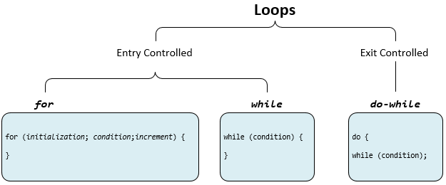
Figure 1: Loops
6.1 for Loop
A for loop is a repetition control structure that allows us to write a loop that is executed a specific number of times. The loop enables us to perform n number of steps together in one line.
Syntax
for (initialization ; condition ; increment) {
// statement block - the body of the loop statements we want to execute
}
If the statement block is only one statement, the braces ({}) are unnecessary.
Although the for allows a number of variables, generally, the initialization sets a loop control variable to its starting value. The condition is usually a relational statement that checks the loop control variable against a termination value and increment increments (or decrements) it. If the condition is false to begin with, the body of the for loop will not execute even once.
How does a for loop execute?
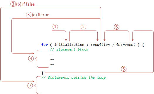
- Control falls into the for loop. initialization is done.
- The flow jumps to the condition.
- Condition is tested.
- The flow goes into the loop's body if the condition yields true.
- If the condition yields false, the flow goes outside the loop (go to step 7).
- The statements inside the body of the loop get executed.
- The flow goes to the increment.
- Updation takes place, and the flow goes to Step 3 again.
- The for loop has ended, and the flow has gone outside.
Flowchart diagram for loop :
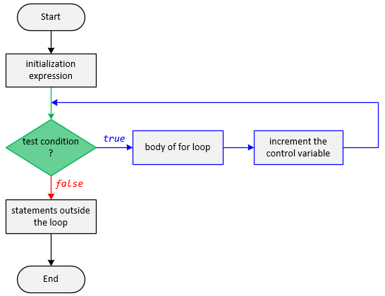
Figure 1.1: The Flowchart of For Loop
Print a String 5 Times using for Loop
This program will try to print "Hello World" 5 times. The program will execute in the following manner:
// C program to illustrate for loop

#include <stdio.h>

int main()
{
    int i = 0;

    // Writing a for loop
    // to print Hello World 5 times
    for (i = 1; i <= 5; i++) {
        printf("Hello World\n");
    }

    return 0;
}
Output
Hello World
Hello World
Hello World
Hello World
Hello World
- Program starts. A variable i is created with an initial value of zero.
- i is initialized with value 1.
- The condition is checked. 1 <= 5 yields true.
- "Hello World" gets printed the 1st time.
- Updation is done. Now i = 2.
- Condition is checked. 2 <= 5 yields true.
- "Hello World" gets printed the 2nd time.
- Updation is done. Now i = 3.
- The condition is checked. 3 <= 5 yields true.
- "Hello World" gets printed the 3rd time
- Updation is done. Now i = 4.
- The condition is checked. 4 <= 5 yields true.
- "Hello World" gets printed for the 4th time
- Updation is done. Now i = 5.
- The condition is checked. 5 <= 5 yields true.
- "Hello World" gets printed for the 5th time
- Updation is done. Now i = 6.
- The condition is checked. 6 <= 5 yields false.
- The flow goes outside the loop to return 0
Multiple Initialization Inside for Loop
We can have multiple initializations in the for loop, as shown below:
for (i = 0, j = 0; i < 25 && j < 25; i++, j++){}
for (i = 1, j = 1 ; i < 13 || j < 15; i++, j++){}
What is the difference between the above for loop and a simple for loop?
- It is initializing two variables that are separated by a comma (,).
- It combines two test conditions using the AND (&&) logical operator. Note: You cannot use multiple test conditions separated by a comma. You must use logical operators such as && or || to join conditions.
- It has two variables in the increment part. Note: Should be separated by a comma.
Benefits of Multiple Initialization
Multiple initialization can make your code more concise and readable. It also allows you to initialize variables that are closely related to each other in a single statement.
Here are some examples of how to use multiple initialization in for loops:
Example 1: Initialize a sum and a product
int i, sum, product;
for (i = 1, sum = 0, product = 1; i < 10; i++) {
    sum += i;
    product *= i;
    printf("sum = %d, product = %d \n", sum, product);
}
Output:
sum = 1, product = 1
sum = 3, product = 2
sum = 6, product = 6
sum = 10, product = 24
sum = 15, product = 120
sum = 21, product = 720
sum = 28, product = 5040
sum = 36, product = 40320
sum = 45, product = 362880
Example 2: Reversing a string
char str[] = "Hello, world!";
char reversedStr[strlen(str) + 1];

for (int i = 0, j = strlen(str) - 1; i < strlen(str); i++, j--) {
    reversedStr[j] = str[i];
}

reversedStr[strlen(str)] = '\0';
printf("The reversed string is: %s\n", reversedStr);
Output:
The reversed string is: !dlrow ,olleH
Example 3: Printing a multiplication table for a given number
int num = 6;

for (int i = 1, result = 0; i < 10; i++) {
  result = num * i;
  printf("%d x %d = %d\n", num, i, result);
}
Output:
6 x 1 = 6
6 x 2 = 12
6 x 3 = 18
6 x 4 = 24
6 x 5 = 30
6 x 6 = 36
6 x 7 = 42
6 x 8 = 48
6 x 9 = 54
Nested For Loop
What is a Nested For Loop?
A nested for loop is a loop that is contained within another loop. The inner loop executes completely for each iteration of the outer loop. Nested loops are commonly used to iterate over two-dimensional arrays, perform nested calculations, and create patterns.
Syntax of a Nested For Loop
for (initialization1; condition1; increment1) {
    for (initialization2; condition2; increment2) {
        // Statements within the inner loop
    }
}
Example 1: Printing a 2D Array
int array[3][3] = {{1, 2, 3}, {4, 5, 6}, {7, 8, 9}};
for (int i = 0; i < 3; i++) {
    for (int j = 0; j < 3; j++) {
        printf("%d ", array[i][j]);
    }
    printf("\n");
}
Output:
1 2 3
4 5 6
7 8 9
In this example, the outer loop iterates three times, corresponding to the rows of the array. The inner loop iterates three times for each iteration of the outer loop, corresponding to the columns of the array.
Example 2: Printing a Triangle Pattern
for (int i = 1; i <= 5; i++) {
    for (int j = 1; j <= i; j++) {
        printf("*");
    }
    printf("\n");
}
Output:
*
**
***
****
*****
Example 3: Finding Prime Factors
int num = 12;
for (int i = 2; i <= num; i++) {
    if (num % i == 0) {
        printf("%d ", i);
        num /= i;
        i--;
    }
}
Output:
2 2 3
In this example, the outer loop iterates from 2 to the input number, representing potential prime factors. The inner loop checks if the input number is divisible by the current factor. If so, it prints the factor and updates the input number accordingly.
Nested for loops are powerful tools for iterating over multiple dimensions or performing nested computations. They are commonly used in various programming tasks and algorithms.
6.2 while loop
While loops are used when we do not know the exact number of loop iterations beforehand, the loop execution is terminated based on test conditions.
The while loop has the general form:
Syntax
while ( condition ) {
// statement block - the body of the loop statements we want to execute
}
- condition: An expression evaluated before each iteration of the loop. If the condition is evaluated to be true, the loop body is executed. If it evaluates to false, the loop terminates.
If a single statement is the object of the while, then the braces ({}) may be omitted. The while loop iterates as long as the condition is true.
The while tests the condition at the top of the loop. Therefore, if the condition is false to begin with, the loop will not execute even once. The condition may be any expression.
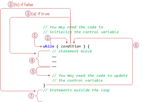
- Control falls into the while loop.
- The flow jumps to the condition.
- Condition is tested.
- If the condition yields true, the flow goes into the Body of the loop.
- If the condition yields false, the flow goes outside the loop (to step 7)
- The statements inside the body of the loop get executed.
- Updation for the control variable.
- Control flows back to Step 2.
- The while loop has ended, and the flow has gone outside.
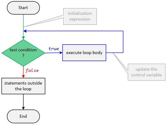
Figure 2.1: The Flowchart of a while Loop
Differences between While Loop and For Loop
Both the while loops and for loops are used for repetitive tasks. However, they differ in their control flow mechanisms:
- For loops: The number of iterations is known beforehand. The loop condition checks for the end of the specified range.
- While loops: The number of iterations is not known in advance. The loop condition determines whether to continue or terminate.
Advantages of While Loops
- Flexibility: They can handle situations where the number of iterations is unknown or determined by the input data.
- Adaptability: They can be used to perform repetitive tasks based on dynamic conditions.
- Versatility: They can be combined with other control flow statements, such as if statements, to create complex control structures.
Applications of While Loops
While loops are widely used in various programming tasks, including:
- Iterating through arrays and data structures
- Performing input validation and error handling
- Implementing menu-driven programs and user interactions
- Simulating real-time processes and event-driven systems
In conclusion, while loops are powerful control flow structures that enable efficient repetition of tasks and dynamic control over program execution. They are essential tools for handling unknown iterations and adapting to changing conditions, making them indispensable for various programming applications.
Print a String 5 Times using while Loop
This program will try to print "Hello World" 5 times. The program will execute in the following manner:
// C program to illustrate while loop

#include <stdio.h>

int main()
{
    // initialization expression
    int i = 1;

    // test expression
    while (i < 6) {
        printf("Hello World\n");

        // update expression
        i++;
    }

    return 0;
}
Output
Hello World
Hello World
Hello World
Hello World
Hello World
- Program starts.
- i is initialized with value 1.
- The condition is checked. 1 < 6 yields true.
- "Hello World" gets printed 1st time.
- Updation is done. Now i = 2.
- The condition is checked. 2 < 6 yields true.
- "Hello World" gets printed 2nd time.
- Updation is done. Now i = 3.
- The condition is checked. 3 < 6 yields true.
- "Hello World" gets printed 3rd time
- Updation is done. Now i = 4.
- The condition is checked. 4 < 6 yields true.
- "Hello World" gets printed 4th time
- Updation is done. Now i = 5.
- The condition is checked. 5 < 6 yields true.
- "Hello World" gets printed 5th time
- Updation is done. Now i = 6.
- The condition is checked. 6 < 6 yields false.
- The flow goes outside the loop to return 0.
Reading Characters until a Newline is Entered
char ch;

while ((ch = getchar()) != '\n') {
    printf("%c", ch);
}
In this example, the loop condition is (ch = getchar()) != '\n', which means the loop will continue to execute as long as the entered character is not a newline ('\n'). The getchar() function reads a character from the input and stores it in the variable ch. The loop body prints the character and then continues to the next iteration. When a newline is encountered, the loop terminates.
6.3 do-while loop
Do-while loops and while loops share similarities but differ in the order of condition evaluation. While loops evaluate the condition before executing the loop body, while do-while loops execute the loop body first and then evaluate the condition. This ensures that the loop body is executed at least once in a do-while loop, regardless of the initial condition.
Syntax
do {
// statement block - the body of the loop statements we want to execute
} while ( condition );
- condition: An expression evaluated after each iteration of the loop. If the condition is evaluated to be true, the loop body is executed again. If it evaluates to false, the loop terminates.
The do-while loop is the only loop in C/C++ that will always have at least one iteration because the condition is tested at the bottom of the loop.
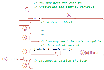
- Control falls into the do-while loop.
- The statements inside the body of the loop get executed.
- You may need to update the control variable
- The flow jumps to the condition.
- The condition is tested:
- If the condition yields true, go to Step 6.
- If the condition yields false, the flow goes outside the loop. (go to Step 7)
- The flow goes back to Step 2.
- The do-while loop has ended, and the flow has gone outside.
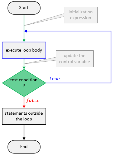
Figure 3.1: The Flowchart of a do-while Loop
Key Difference from While Loop
The do-while loop differs from the while loop in the order of condition checking. In a while loop, the condition is checked before entering the loop, and the loop body is executed only if the condition is true. In a do-while loop, the loop body is executed first, and the condition is checked after each iteration. This guarantees that the loop body is executed at least once.
Advantages of Do-While Loops
- Guaranteed Execution: They ensure that the loop body is executed at least once, regardless of the initial condition.
- Useful for Input Validation: They can be used to perform input validation and repeat the input process until a valid input is received.
- Handling Unknown Iterations: They can be used when the number of iterations is unknown or determined by the input data.
Applications of Do-While Loops
Do-while loops are commonly used in various programming scenarios, including:
- Input validation and error handling
- Menu-driven programs and user interactions
- Implementing loops with unknown termination conditions
- Performing iterative tasks that require at least one execution
Do-while loops provide a valuable addition to the control flow repertoire of C and C++ programmers. Their ability to guarantee at least one execution of the loop body makes them particularly useful for input validation, handling unknown iterations, and performing tasks that require at least one execution. By understanding their syntax and applications, programmers can effectively utilize do-while loops to enhance their programs and achieve desired outcomes.
Print a String using do-while Loop
This program will try to print "Hello World". The program will execute in the following manner:
// C program to illustrate do-while loop

#include <stdio.h>

int main()
{
    // initialization expression
    int i = 2;

    do {
        // loop body
        printf("Hello World\n");

        // update expression
        i++;
    // test expression
    } while (i < 1);

    return 0;
}
Output
Hello World
- Program starts.
- i is initialized to 2.
- Execution enters the loop.
- "Hello World" gets printed 1st time.
- Updation is done. Now i = 2.
- Condition is checked. 2 < 2 yields false.
- The flow goes outside the loop to return 0.
Guessing a Secret Number
int secretNumber = 5;
int guess;

do {
    printf("Enter your guess: ");
    scanf("%d", &guess);

    if (guess == secretNumber) {
        printf("Congratulations! You guessed the correct number.\n");
        break;
    } else if (guess > secretNumber) {
        printf("Your guess is too high. Try again.\n");
    } else {
        printf("Your guess is too low. Try again.\n");
    }
} while (guess != secretNumber);
In this example, the do-while loop ensures that the user is prompted to enter a guess at least once. The loop continues to execute as long as the guess does not equal the secret number. Once the correct guess is entered, the loop terminates.
Reading Characters until a Space is Entered
char ch;

do {
  ch = getchar();
  printf("%c", ch);
} while (ch != ' ');
In this example, the do-while loop ensures that at least one character is read from the input. The loop continues to execute as long as the entered character is not a space (' '). Once a space is encountered, the loop terminates.
6.4 Infinite Loop
An infinite loop (sometimes called an endless loop ) is a piece of coding that lacks a functional exit so that it repeats indefinitely. An infinite loop occurs when a condition is always evaluated to be true.
Most of the time, we create infinite loops by mistake. However, this doesn't mean that the infinite loops are not useful. Infinite loops are commonly used in programs that keep running for long periods of time until they are stopped, like the webserver.
| Harm Caused by Infinite Loops | Description |
| Excessive Processor Usage | Infinite loops continuously execute without termination, relentlessly consuming processor resources. This can lead to system slowdown, unresponsiveness, and increased power consumption. |
| Memory Consumption | In C and C++, infinite loops can cause memory leaks. This occurs when memory is allocated within the loop but never released. As the loop continues to execute, the allocated memory remains in use, gradually depleting the available RAM. This can lead to out-of-memory errors, system crashes, and complete system failure. |
Excessive Processor Usage
Infinite loops can significantly impact a system's performance due to their relentless consumption of processor resources. As the loop continuously executes without termination, it demands a constant allocation of processor time and power, leading to several detrimental effects:
- System Slowdown: The excessive processor usage caused by an infinite loop can severely hinder the system's overall performance. Other processes and applications competing for processor resources will experience delays and sluggishness, making the entire system feel unresponsive and slow.
- Unresponsiveness: In extreme cases, an infinite loop can monopolize the processor, preventing other essential system processes from executing. This can result in a completely unresponsive system, where the user cannot interact or perform any actions.
- Increased Power Consumption: The continuous execution of an infinite loop translates to increased power consumption, leading to faster battery depletion in laptops and mobile devices. Additionally, the generated heat from the overworked processor can contribute to overheating issues.
Memory Consumption
In C and C++, infinite loops can seriously threaten memory management, leading to memory leaks and potential system crashes. Memory leaks occur when memory is allocated within the loop but never released, even after the loop has finished executing. This unmanaged memory remains in use, gradually depleting the available RAM. As the memory consumption grows, the system can experience:
- Out-of-Memory Errors: When the system runs out of available RAM due to the accumulated memory leaks caused by infinite loops, it will throw out-of-memory errors. These errors indicate that the system cannot allocate the necessary memory for new processes or operations.
- System Crashes: As the memory leaks from infinite loops continues to consume RAM, the system may eventually reach a point where no more memory is available. This can trigger system crashes, causing the system to shut down or become unusable abruptly.
- Complete System Failure: In severe cases, the memory leaks caused by infinite loops can lead to complete system failure. This occurs when the system's critical processes cannot allocate the required memory, rendering the system inoperable.
Intentional Infinite Loops
While infinite loops are generally considered errors in programming, there are some instances where they are intentionally used for specific purposes. These intentional infinite loops are carefully designed to serve specific functionalities and are not a result of programming mistakes.
Purpose of Intentional Infinite Loops
- Embedded Systems: In embedded systems, infinite loops are often used to maintain a continuous program execution, ensuring that the system remains active and responsive to external events. For example, an embedded controller for a sensor might continuously read sensor data and update its output based on the readings.
- Event-Driven Systems: In event-driven systems, infinite loops are employed to wait for and respond to incoming events. These loops continuously monitor for user input, network messages, or other triggers and execute the appropriate actions when events occur.
- Background Processes: Infinite loops can be used to run background processes that operate independently of the main program flow. These processes might perform ongoing tasks like monitoring system resources, handling asynchronous operations, or maintaining system stability.
- Menu-Driven Programs: In menu-driven programs, infinite loops are often used to present a menu and handle user interactions. The loop continuously displays the menu options, accepts user input, and executes the corresponding actions until the user chooses to exit the program.
- Game Development: In game development, infinite loops are commonly used to control the game loop, which is responsible for updating the game state, rendering graphics, and handling player input. The game loop continuously runs until the game ends, ensuring a smooth and responsive gaming experience.
Examples of Intentional Infinite Loops
Embedded Sensor Controller
while (1) {
    sensorValue = readSensorData();
    updateOutput(sensorValue);
}
This loop continuously reads sensor data and updates the system output accordingly, ensuring that the embedded controller remains active and responsive to sensor changes.
Event-Driven Network Listener
while (1) {
    if (receiveMessage()) {
        processMessage(message);
    }
}
This loop continuously monitors for incoming network messages. When a message is received, it is processed and the appropriate actions are taken.
Background Resource Monitor
while (1) {
    checkSystemResources();
    if (resourcesLow()) {
        takeCorrectiveActions();
    }
}
This loop continuously monitors system resources and takes corrective actions if resources are running low.
Game Loop
while (1) {
    updateGameState();
    renderGraphics();
    handleUserInput();
}
This loop continuously updates the game state, renders the game graphics, and handles player input, ensuring a smooth and responsive gaming experience.
Remember, intentional infinite loops should be used with caution and only when absolutely necessary. They require careful design and implementation to avoid unintended behavior and ensure the stability and performance of the program.
Infinite Loops by Mistake
Infinite Loops by Mistake
The reason behind the occurrence of an Infinite loop
Generally, six reasons become the reason behind the occurrence of an infinite loop.
- No terminating condition.
- Having one condition that can never be met.
- Having a condition that causes the loop to start again and again.
- Miss the incrementer or decrementer (if your logic needs one)
- Continue statement in the wrong place (if your logic needs one)
- Wrong comparisons in loop condition (less than or greater mixed up)
So whenever you get an infinite loop, check from these six conditions. There is a high chance that you'll get your mistake.
In the following examples, we demonstrate what kind of mistakes can lead to an infinite loop:
Impossible termination condition
An example for loop in C:
unsigned int i;
for (i = 1; i != 0; i++) {
// loop code
}
It appears that this will go on indefinitely, but in fact, the value of i will eventually reach the maximum value storable in an unsigned int and adding 1 to that number will wrap-around to 0, breaking the loop. The actual limit of i depends on the details of the system and compiler used. With arbitrary-precision arithmetic, this loop would continue until the computer's memory could no longer hold i. If i was a signed integer, rather than an unsigned integer, overflow would be undefined. In this case, the compiler could optimize the code into an infinite loop.
Mathematical errors
Here is one example of an infinite loop in C:
int x;
while (x < 5) {
x = 1;
x = x + 1;
}
This creates a situation where x will never be greater than 5, since at the start of the loop code x is given the value of 1, thus, the loop will always end in 2 and the loop will never break. This could be fixed by moving the x = 1 instruction outside the loop. Essentially what this infinite loop does is to instruct a computer to keep on adding 1 to 1 until 5 is reached. Since 1 + 1 always equals 2, this will never happen.
Assignment Operator in Condition Expression
Another common mistake that leads to an infinite loop is to use the assignment operator (=) where the equality operator is needed (==). For example, here is a snippet in C:
#include <stdio.h>
int main(void)
{
int a = 0;
while (a < 10) {
printf("%d\n", a);
if (a = 5)
printf("a equals 5!\n");
a++;
}
return 0;
}
The expected output is the numbers 0 through 9, with an interjected "a equals 5" between 5 and 6. However, in the line "if (a = 5)" above, the programmer has confused the = (assignment) operator with the == (equality test) operator. Instead, this will assign the value of 5 to a at this point in the program. Thus, a will never be able to advance to 10, and this loop cannot terminate.
Variable handling errors
Unexpected behavior in evaluating the terminating condition can also cause this problem. Here is an example (in C):
float x = 0.1;
while (x != 1.1) {
printf("x = %f\n", x);
x += 0.1;
}
On some systems, this loop will execute ten times as expected, but on other systems, it will never terminate. The problem is that the loop terminating condition (x != 1.1) tests for exact equality of two floating-point values, and the way floating-point values are represented in many computers will make this test fail because they cannot represent the value 0.1 exactly, thus introducing rounding errors on each increment (the x += 0.1 statement).
Forget to Update Control Variable
int i = 1;
while(i < 10) {
printf("%d\n", i);
}
Here, we are not updating the value of i. So, after each iteration, the value of i remains the same. As a result, the condition (i < 10) will always be true. For the loop to work correctly, add i++; just after the printf() statement.
Always remember it is easier to forget the update expression in the while and do-while loop than in the for loop.
Condition Never Be Ture
short int i;
for (i = 32765; i < 32768; i++) {
printf("%d\n", i);
}
This loop is an infinite loop. Here is why. According to the condition, the loop will execute until (i < 32768). Initially, the value of i is 32765 and after each iteration, its value is incremented by the update expression (i++). But the value of short int type ranges from -32768 to 32767. If you try to increment the value of i beyond 32767, it goes on the negative side and this process keeps repeating indefinitely. Hence the condition (i < 32768) will always be true.
Float-Pointer Number
float f = 2;
while(f != 3.0)
{
printf("%f\n", f);
f += 0.1;
}
This loop is infinite because computers represent floating-point numbers as approximate numbers, so 3.0 may be stored as 2.999999 or 3.00001. So, the condition (f != 3.0) never becomes false. To fix this problem, write the condition as (f <= 3.0).
Semicolon at Wrong Place
int i = 0;
while(i <= 5);
printf("%d\n", i);
This loop will produce no output and will go on executing indefinitely. Take a closer look and notice the semicolon (;) at the end of the while condition. We know the semicolon (;) after the condition is a null statement. So, the loop is equivalent to the following:
int i = 0;
while(i <= 5) {
; // a null statement
}
printf("%d\n", i);
We can now clearly see that we are not updating the value i inside the while loop. As a result, it will go on executing indefinitely.
Alderson loop
The term "Alderson loop" is a slang or jargon term for an infinite loop in C or C++ where an exit condition is available but inaccessible in the current code implementation. This typically occurs due to a programmer's error that prevents the loop from terminating properly.
Alderson loops are often encountered in user interface (UI) code, where they can cause modal dialog boxes or other UI elements to remain permanently visible, blocking user interaction and rendering the program unresponsive. These loops can be particularly frustrating to debug as the correct exit condition is not utilized correctly.
To identify Alderson loops, programmers should carefully examine the loop logic and look for potential errors that could prevent the loop from terminating. Common causes of Alderson loops include:
- Missing or Incorrect Termination Condition: The loop may lack a proper exit condition, or the condition may not be evaluated correctly, preventing the loop from ever ending.
- Invalid Loop Updates: The loop may update variables or data structures in a way that never allows the exit condition to become true, effectively trapping the loop in an endless cycle.
- Condition Overrides: Other parts of the code may override the loop's exit condition, preventing it from taking effect and causing the loop to continue indefinitely.
- Error Handling Issues: Improper error handling mechanisms may prevent the loop from exiting when errors occur, leading to an infinite loop situation.
- User Input Issues: In UI code, invalid user input or unexpected input values may not be handled correctly, causing the loop to get stuck in an endless cycle.
To avoid Alderson loops, programmers should adhere to sound coding practices, thoroughly review their code for potential errors, and employ rigorous testing and debugging techniques. Additionally, using proper error-handling mechanisms and validating user input can help prevent these loops from occurring in the first place.
The following C code example of an Alderson loop, where the program is supposed to sum numbers given by the user until zero is given, but where the programmer has used the wrong operator:
sum = 0;
while (true) {
printf("Input a number to add to the sum or 0 to quit");
i = getUserInput();
if (i * 0) { // if i times 0 is true, add i to the sum.
// Note: ZERO means FALSE, Non-Zero means TRUE. "i * 0" is ZERO (FALSE)!
sum += i; // sum never changes because (i * 0) is 0 for any i;
// it would change if we had != in the condition instead of *
}
if (sum > 100) {
break; // terminate the loop; exit condition exists but is never reached because sum is never added to
}
}
Infinite Loop with Condition Override
int i = 0; while (i < 10) {
printf("%d\n", I);
i++;
if (i == 5) {
i = 0; // Condition override
}
}
In this example, the statement i = 0; inside the loop overrides the loop's exit condition. This prevents the loop from terminating when i reaches 5, causing it to continue indefinitely.
Infinite Loop with Error Handling Issue
int i = 0;
while (i < 10) {
printf("%d\n", I);
i++;
if (openFile("data.txt") != 0) {
continue; // Error handling issue
}
// Process data from the file
}
In this example, the error handling mechanism using continue; is flawed. When openFile() fails, the loop skips to the next iteration instead of terminating. This causes the loop to continue executing indefinitely, even though the file could not be opened.
Infinite Recursion
Infinite recursion is a special case of an infinite loop that is caused by recursion. The following example in C returns a stack overflow error:
void test1()
{
test1();
}
int main()
{
test1();
}
Difference between for and while loop in C/C++
| for Loop | while Loop |
|---|---|
| Initialization may be either in the loop statement or outside the loop. | Initialization is always outside the loop. |
| Once the statement(s) is executed then after increment is done. | The increment can be done before or after the execution of the statement(s). |
| It is normally used when the number of iterations is known. | It is normally used when the number of iterations is unknown |
| Condition is a relational expression. | The condition may be an expression or non-zero value. |
| It is used when initialization and increment are simple. | It is used for complex initialization. |
| The for is entry controlled loop. | The while is also entry controlled loop. |
| for ( init ; condition ; increment ) { statement(s); } |
while ( condition ) { statement(s); } |
Difference between for and do-while loop in C/C++
| for Loop | do-while Loop |
|---|---|
| Statement(s) is executed once the condition is checked. | Condition is checked after the statement(s) is executed. |
| It might be that statement(s) gets executed zero times. | Statement(s) is executed at least once. |
| For the single statement, the bracket is not compulsory. | Brackets are always compulsory. |
| Initialization may be outside or in the condition box. | Initialization may be outside or within the loop. |
| for loop is entry controlled loop. | do-while is exit controlled loop. |
| for ( init ; condition ; increment) { statement(s); } |
do { statement(s); } while ( condition ); |
Difference between while and do-while loop in C/C++
| while Loop | do-while Loop |
|---|---|
| The condition is checked first, and then the statement(s) is executed. | Statement(s) is executed at least once; thereafter, the condition is checked. |
| It might occur that the statement(s) is executed zero times if the condition is false. | At least once the statement(s) is executed. |
| No semicolon at the end of the while. while (condition) |
A semicolon at the end of the while. do { } while(condition); |
| If there is a single statement, brackets are not required. | Brackets are always required. |
| The variable in the condition is initialized before the execution of the loop. | The variable may be initialized before or within the loop. |
| while loop is an entry-controlled loop. | The do-while loop is an exit-controlled loop. |
| while (condition) { statement(s); } |
do { statement(s); } while (condition); |
Summary
- Use for loop when the number of iterations is known beforehand, i.e. the number of times the loop body is needed to be executed is known.
- Use while loops where the exact number of iterations is not known, but the loop termination condition is known.
- Use do-while loop if the code needs to be executed at least once like in Menu-driven programs
Questions
- Binary and Hexadecimal: Input an unsigned 8-bit integer (uint8_t) and display its binary and hexadecimal value on the screen. (Using shifter and bitmask to get all digits from left to right).
- Use for loops to construct a program that displays the following pattern on the screen:
-
X
XX
XXX
XXXX
XXXXX
-
X
XX
XXX
XXXX
XXXXX
-
X
XXX
XXXXX
XXXXXXX
XXXXXXXXX
For (b), (c), (d), (e), and (f), one way to do this is to nest two inner loops, one to print spaces and one to print Xs, inside an outer loop that steps down the screen from line to line.-
XXXXXXXXX
XXXXXXX
XXXXX
XXX
X
-
X
XXX
XXXXX
XXXXXXX
XXXXXXXXX
XXXXXXX
XXXXX
XXX
X
-
X
XX
XXX
XXXX
XXXXX
XXXX
XXX
XX
X
-