KB07: Build the Test Circuit Component and Jumper Layout
Introduction
Part A: Parts and Tools
This lab involves designing, building, and testing circuits using design concepts from the Digital Logic course EE-2440. You should have a lab kit box containing parts and equipment for the duration of the semester. The equipment includes:
- Breadboard (also referred to as a protoboard) where you will build your circuits. In the lab room, the breadboard should come with a test circuit and already connected. If you are taking an online lab course, you must build the test circuit on the breadboard first.
- Several cables (for use with power supply and oscilloscope).
- Wire cutter/stripper tool for cutting wire and stripping the ends for insertion in the breadboard.
- IC (integrated circuit) chips for building circuits you design in the various experiments.
- Logic probe: this is the main tool you will use in the lab for troubleshooting your designs.
If you are taking the on-campus lab, you must have the following additional items:
- USB flash drive: you'll need to store waveform data captured on the oscilloscope screen and transfer it to a PC.
- Lab Journal: you'll need to purchase a composition book to record your prelab work (design work including truth tables, K-maps, state tables, state machines, logic diagrams, and wiring diagrams), your lab experimental results (including your observations, results – waveforms, truth tables, and state tables/machines), answers to any questions posed in the lab manual, and any note that you take related to the experiments.
Part B: Circuit Diagrams
Your circuit diagrams should serve two functions:
- Logic Diagram — to show the flow of logic in your design.
- Wiring Diagram — to guide you in making circuit connections.
It is recommended that you draw your circuit diagrams directly in your lab journal. However, when you submit a laboratory report, you'll need schematic capture software to clearly and neatly draw circuit diagrams. You will be responsible for submitting typed laboratory reports for experiments 3, 5, 6, 7, and 10.
For your laboratory reports, use one of the "schematic capture" programs to draw the schematic diagram:
- KiCad (a part of ExpressPCB) to draw your circuit diagrams: https://www.expresspcb.com/
- KiCad EDA (a cross-platform and open-source Electronics Design Automation suite): https://KiCad.org
Download and install the schematic software early in the semester — you'll need it starting with Lab 2.
With KiCad, the following requirements will be easy to meet:
- To make circuit logic as clear as possible, gate and flip-flop symbols should be shown separately — not together inside a chip rectangle as they are shown at the end of this manual. That
way, they can be placed individually in a diagram wherever it is convenient. Only when a chip acts as a single unit (counter, MUX, etc.), not a collection of identical elements, is represented as a rectangle.
The unit is shown as a rectangle (counter, MUX), pins are not shown in their true positions around the rectangle. Instead, they are arranged to make the logic flow easy to follow, with logic inputs at the left and outputs at the right. Control inputs (e.g., clock, reset, enable) can appear at the left or the top or bottom of the rectangle. - Active-low inputs and outputs are shown with small inverting circles. Alternatively, a bar above a variable's name or a forward slash before it (i.e.,/X) indicates inverted logic. These symbols are very helpful when following logic flow or troubleshooting a design.
- In all rectangles, pin names (e.g., D, Q for flip-flops, Cin for adders, Clk for counters, etc.) are shown inside, pin number outside. Chip part numbers are placed next to the device symbols (e.g., 7432 next to an OR-gate symbol).
- Each rectangle and gate symbol should contain a "U" (Unit) number. In the case of gates and flip-flops, these unit numbers identify which chip they are part of. Suppose your design involves six 2-input NAND gates, four gates to a chip. You will need two 7400 chips. Suppose you number these U2 and U3. Then four gate symbols might be designated U2, the other two U3. A connecting wire from pin 3 of U2 to pin 9 of U3 could then be described as "U2-3 to U3-9". A number system such as this will do much to speed up the troubleshooting process. One partner can call out each connection from the diagram, while the other partner checks the circuit to see if the connection has been correctly made.
- Your circuit will be laid out as a line of chips (with spaces between so you can lever a chip out if it needs replacing). All chips will be facing the left, as shown in the diagram on the next page. In your diagram, label the left-most chip U1. Then the next chip from the left would be U2, etc. This will make it easy to associate chip components (like gates) on the diagram with the physical chip on the board.
Different gates or flip-flops within a chip can be assigned a different label, e.g., A, B, C., etc. Suppose the first chip on the left is a 7474, which you label unit 1 (U1) on the diagram. Now, 7474's have two D flip-flops. Thus, U2A could refer to one flip-flop, and U2B could refer to the other flip-flop. However, the flip-flops can also be told apart because they each have different pin numbers, so the labels A, B, etc., aren't really necessary. Make sure when drawing a diagram that no two gates or flip-flops show the same pin numbers unless they belong to different chips. Later, when connecting your circuit, make sure you use the same pin numbers as shown in your diagram.
Part C.1: Test Circuit (For On-Campus Lab Course)
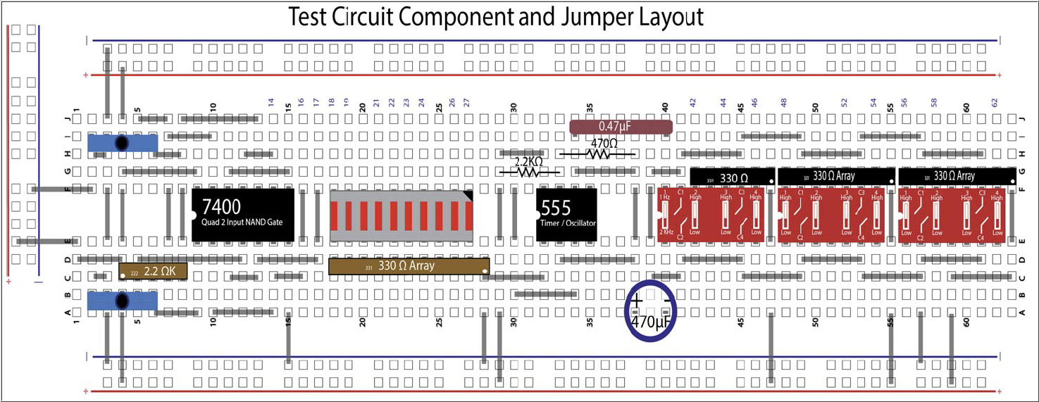
Figure 7.1: Test Circuit Component and Jump Layout Diagram
Figure 7.1 is a layout diagram of the circuit to be used in testing your experimental designs. If you are taking an on-campus lab course, each group should have a breadboard that comes with a connected test circuit in the locker. Please check the connections on the breadboard, and make sure all the connections are correct.
If you are taking an at-home lab course, you have to build Clock and Digital Outputs circuits on your breadboard.
The test circuit consists of the following sections (starting at the left side of the layout diagram in Figure 7.1):
- Pulser Debouncer Circuit
- LED Bargraph Display
- Clock
- Digital Outputs
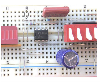
Pulser Circuitry
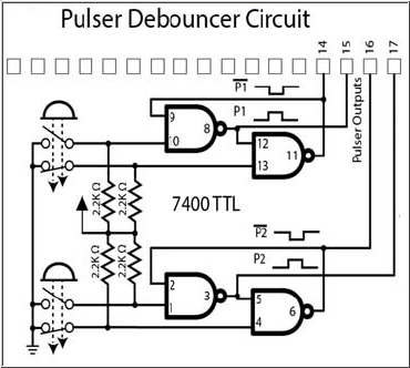
Figure 7.2: Pulser Debouncer Circuit Diagram
There are two pushbutton switches, each having normally open and normally closed contacts. The outputs of each switch are sent through a NAND debouncing circuit, and the NAND outputs are identified as "normally low" and "normally high".

In this case, "normally" means when the button is not being pressed. When the button is pressed, the normally-low output goes high, and the normally-high output goes low. When the button is released, the outputs return to their normal levels.
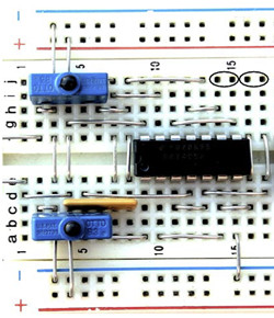
The photo at the right of the two pulsers (push-button)\ switches) and the 7400 NAND chip that denounces their outputs. These outputs (also shown in Figure 7.2) are circled: the two holes at rows 14 and 15 are denounced output of the top pulser; those at rows 16 and 17 are of the lower pulser. (Each pair consists of normally high and normally low output.)
When a pulser is pressed, its metal contacts come together and, because of their springiness, their voltages initially "bounce", as shown: ![]() or
or ![]()
Because of this behavior, the direct output of the pulsers can not be used to clock a counter or flip flop chip since one press of a pulser results in many pulses (more than shown here). So the outputs are brought to a 4-NAND 7400 chip. The gates are connected as two latches. As soon as a pulser output changes level, the latch output flips accordingly and the bounces that follow are ignored: ![]()
![]()
LED Display
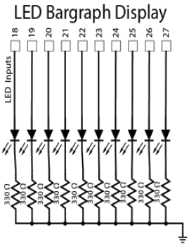
Figure 7.3: LED Bargraph Display Diagram
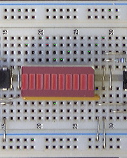
There is a 10-LED "bargraph" chip next to the NAND chip. It should be inserted into the board with the small corner notch at the upper right (as shown in Figure 7.1). The chip voltages you wish to display are brought to LED inputs (above the LED chip in the diagram). When a voltage goes high, current flows down through an LED and then into one end of a SIP resistor. The other end of the resistor, in common with all the others in the SIP, is connected to the ground (blue) strip at the bottom of the circuit.
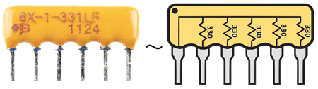
"SIP" Resistor Array
SIP (Single In-line Package — only one row of pins) used in this lab varies in color and number of pins. In this example, it has 6 pins but only 5 resistors. The pin at the end marked with a dot is the "common". For this circuit, the common is connected to 0V (ground) while the pins in the resistive legs are brought to the cathodes of the LEDs. A marking like 331 means \(33 \times {10^1} = 330\Omega \) for each resistor. (Similarly, 103 would mean \(10 \times {10^3} = 10K\Omega \))
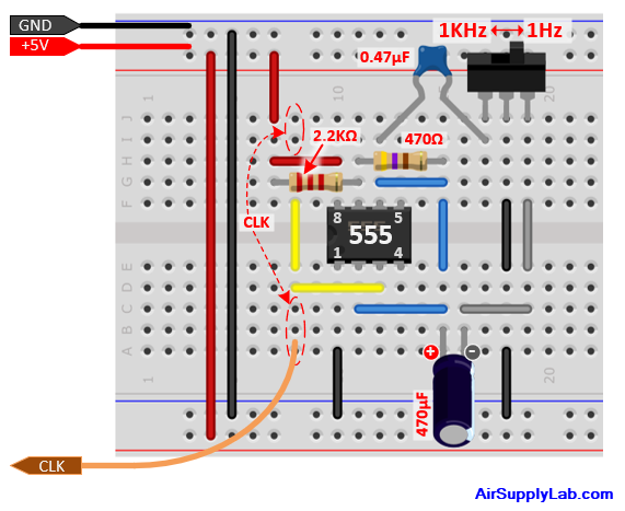
Free-Running Clock
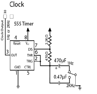
The 555 timer chip is connected as an oscillator. The oscillation frequency is determined by an RC circuit. There are two R's, a 2.2KΩ and a 470Ω, and there is a choice of two capacitors: C1 = 0.47 μF and C2 = 470 μF (μ = micro = 10-6). Whichever capacitor is chosen, it is charged up to a maximum through the two R's in series, 2,670 Ω, but discharged down to a minimum through the 470Ω alone. While the capacitor is being charged, the timer output is high; while it is being discharged, the output is low. Since charge and discharge times depend on circuit resistance, the output is high much longer than it is low resulting in an unsymmetrical rectangular ![]() waveform. (This can be seen by displaying the timer output on an oscilloscope.)
waveform. (This can be seen by displaying the timer output on an oscilloscope.)
Note: C2 is an electrolytic capacitor, it is "polarized"; i.e. it has a positive and a negative terminal. The voltage at the positive lead must always be greater than that at the negative. There is a stripe down the side of the capacitor indicating the side with the negative lead. For a cylinder-shaped radial capacitor, the negative lead will also be shorter than the positive. This attention to polarity is necessary since if the electrolytes are inserted backward, they can rupture or even explode.
The left-most toggle switch allows you to switch between C1 and C2. Since C2 is larger than C1 by a factor of 1,000, switching from C1 to C2 will lower the clock frequency by the same factor. Thus C1 selects the high-frequency range ![]() , and C2 selects the low-frequency range
, and C2 selects the low-frequency range ![]() . With C1 in the circuit, the frequency will be approximately 1,000 Hz (1 KHz), while with C2, the frequency will be around 1 Hz. The timer output will be used to clock a counter chip (the 7493) and D and JK flipflop chips (7474 and 7476).
. With C1 in the circuit, the frequency will be approximately 1,000 Hz (1 KHz), while with C2, the frequency will be around 1 Hz. The timer output will be used to clock a counter chip (the 7493) and D and JK flipflop chips (7474 and 7476).
The high-frequency clock (using C1) is provided for testing circuits with a scope. Its period is about 1 msec (1/1000 sec) which corresponds to one horizontal division on the scope screen when using the 1 msec/cm setting. Don't try to display high-frequency voltage changes using LEDs; the changes are too fast for the eye to see. In contrast, display low-frequency voltage changes (using C2) with the LEDs rather than the scope.
Also, when troubleshooting a circuit that is not working properly, it is usually better to disconnect the clock from the 555 timer and use a pulser instead. The problem with using the 555 clock is that you can't stop it when you want to freeze circuit operation so you can check for connection errors with a logic probe.
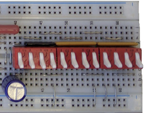
Toggle (DIP) Switches
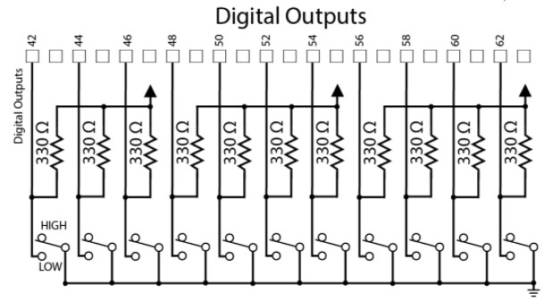
To the right of the toggle switch that selects between C1 and C2, there are 11 more toggle switches. Switch outputs are found in the holes so marked on the layout diagram. Each output is adjacent to a 330Ω pull-up resistor. When a switch is open (up), its output voltage is "pulled up" to 5V by the resistor. (With the switch open, no current flows through the resistor, so the voltage at its lower end is the same as at its upper end; i.e. 5V.) When the switch is closed (down), it connects the lower end of the resistor to the ground, so the switch output voltage falls to 0V.
Part C.2: Test Circuit (For the Online Lab Course)
If you are taking this lab as an online lab course, you have to build a clock generator circuit on the breadboard.